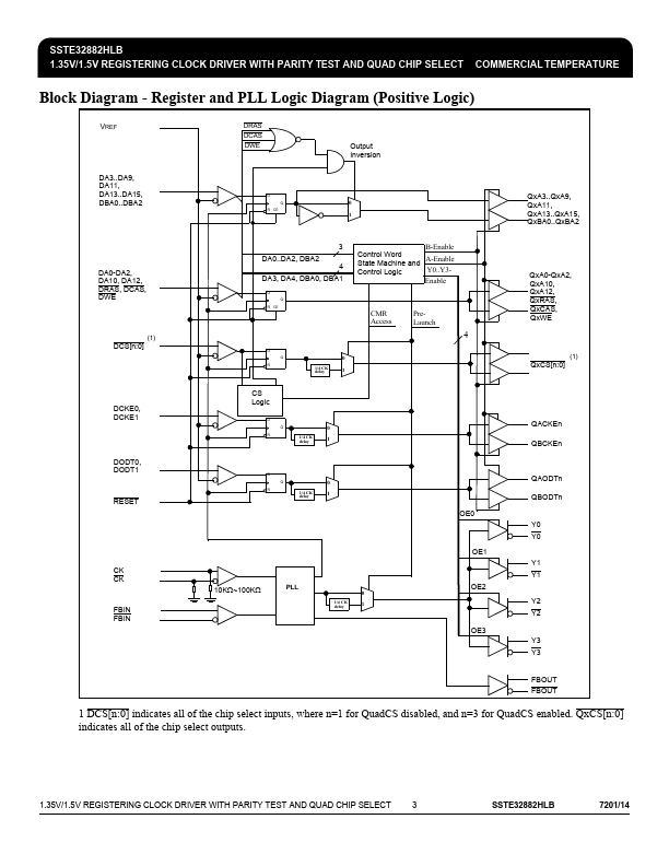
Datasheet4U Logo Datasheet4U.com

SSTE32882HLB Datasheet 1.35V/1.5V REGISTERING CLOCK DRIVER

Manufacturer: IDT

Datasheet Details

Part number SSTE32882HLB
Manufacturer IDT
File Size 1.22 MB
Description 1.35V/1.5V REGISTERING CLOCK DRIVER
Datasheet download datasheet SSTE32882HLB Datasheet

General Description

This 28-bit 1:2, or 26-bit 1:2 and 4-bit 1:1, registering clock driver with parity is designed for 1.35V and 1.5V VDD operation.

All inputs are 1.35V and 1.5V CMOS compatible, except the reset (RESET) and MIRROR inputs which are LVCMOS.

All outputs are 1.35V and 1.5V CMOS edge-controlled drivers optimized to drive single terminated 25 to 50 traces in DDR3 RDIMM applications, except the open-drain error (ERROUT) output.

Overview

DATASHEET 1.35V/1.5V REGISTERING CLOCK DRIVER WITH PARITY TEST AND QUAD CHIP SELECT.

Key Features

  • Pinout optimizes DDR3 RDIMM PCB layout.
  • 1-to-2 Register Outputs and 1-to-4 Clock Pair Outputs support stacked DDR3 RDIMMs.
  • Phase Lock Loop clock driver for buffering one differential clock pair (CK and CK) and distributing to four differential outputs.
  • Supports LVCMOS switching levels on the RESET and MIRROR inputs.
  • Checks priority on DIMM-independent data inputs.
  • Supports dynamic 1T/3T timing transaction and output inversion feature for imp.