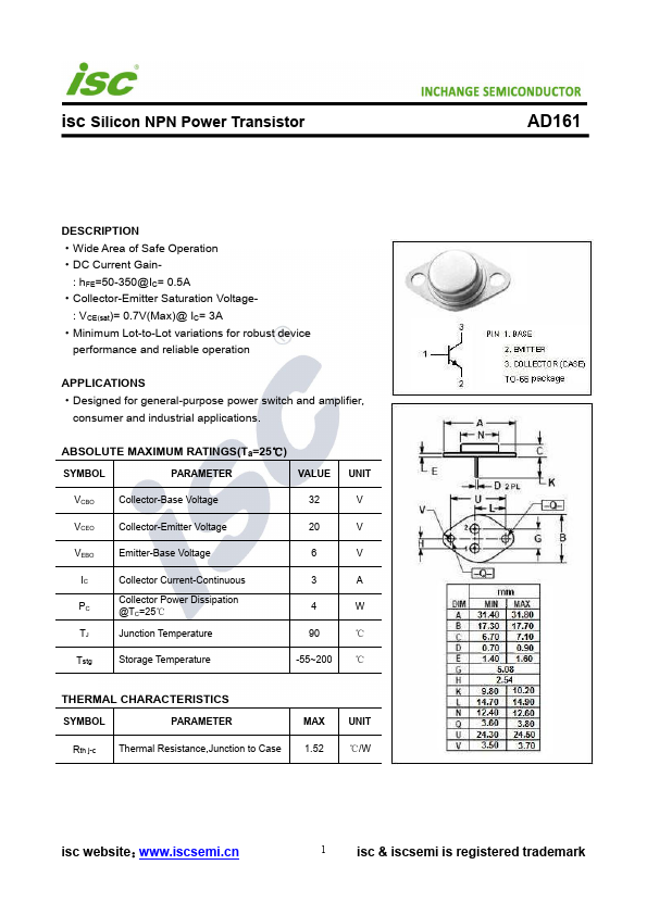
Datasheet4U Logo Datasheet4U.com

AD161 - NPN Transistor

General Description

·Wide Area of Safe Operation ·DC Current Gain- : hFE=50-350@IC= 0.5A ·Collector-Emitter Saturation Voltage- : VCE(sat)= 0.7V(Max)@ IC= 3A ·Minimum Lot-to-Lot variations for robust device performance and reliable operation APPLICATIONS ·Designed for general-purpose power switch and amplifier, consumer and industrial applications.

ABSOLUTE MAXIMUM RATINGS(Ta=25℃) SYMBOL PARAMETER VALUE UNIT VCBO Collector-Base Voltage 32 V VCEO Collector-Emitter Voltage 20 V VEBO Emitter-Base Voltage 6 V IC Collector Current-Continuous PC Collector Power Dissipation @TC=25℃ TJ Junction Temperature 3 A 4 W 90 ℃ Tstg Storage Temperature -55~200 ℃ THERMAL CHARACTERISTICS SYMBOL PARAMETER Rth j-c Thermal Resistance,Junction to Case MAX 1.52 UNIT ℃/W isc website:www.iscsemi.cn 1 isc & iscsemi is registered trademark isc Silicon NPN Power Transistor ELECTRICAL CHARACTERISTICS Tj=25℃ unless otherwise specified SYMBOL PARAMETER CONDITIONS V(BR)CEO Collector-Emitter Breakdown Voltage IC= 100mA ;

IB= 0 V(BR)CBO Collector-Base Breakdown Voltage IC= 1mA ;

Overview

isc Silicon NPN Power Transistor AD161.