Inchange Semiconductor SPW35N60C3
N-Channel MOSFET
| Part No. | SPW35N60C3 |
|---|---|
| Datasheet | SPW35N60C3 Download |
| Manufacturer |  Inchange Semiconductor |
| Description | N-Channel MOSFET |
| Buy | Stock & Price |
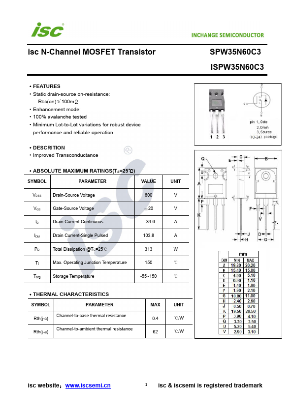
FEATURES
●Static drain-source on-resistance: RDS(on)≤100mΩ●Enhancement mode:
●100% avalanche tested
●Minimum Lot-to-Lot variations for robust device performance and reliable operation
●DESCRITION
●Improved Transconductance
●
ABSOLUTE MAXIMUM RATINGS
(Ta=25℃) SYMBOL PARAMETER VALUE VDSS Drain-Source Voltage 600 VGS Gate-Source Voltage ±20 ID Drain Current-Continuous 34.6 IDM Drain Current-Single Pulsed 103.8 PD Total Dissipation @TC=25℃ 313 Tj Max. Operating Junction Temperature 150 Tstg Storage Temperature -55~150 UNIT V V A A W ℃ ℃●THERMAL CHARACTERISTICS SYMBOL PARAMETER Rth(j-c) Channel-to-case thermal resistance Rth(j-a) Channel-to-ambient thermal resistance MAX 0.4 62 UNIT ℃/W ℃/W SPW35N60C3 ISPW35N60C3 isc website: 1 isc & iscsemi is registered trademark isc N-Channel MOSFET Transistor
ELECTRICAL CHARACTERISTICS
TC=25℃ unless otherwise specified SYMBOL PARAMETER CONDITIONS BVDSS Drain-Source Breakdown Voltage VGS=0V; ID=0.25mA VGS(th) Gate Threshold Voltage VDS=VGS; ID=1.9mA RDS(...