International Rectifier IRF40B207
Power MOSFET
| Part No. | IRF40B207 |
|---|---|
| Datasheet | IRF40B207 Download |
| Manufacturer |  International Rectifier |
| Description | Power MOSFET |
| Buy | Stock & Price |
ELECTRICAL CHARACTERISTICS
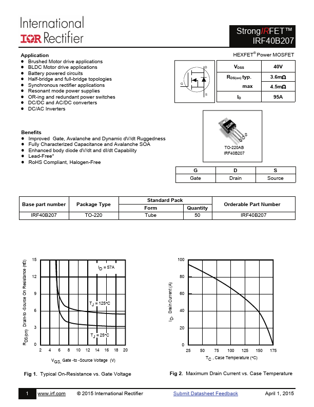
@ TJ = 25°C (unless otherwise specified) Symbol Parameter Min. Typ. Max. Units Conditions gfs Qg Qgs Qgd Qsync td(on) tr td(off) tf Forward Transconductance Total Gate Charge Gate-to-Source Charge Gate-to-Drain Charge Total Gate Charge Sync. (Qg– Qgd) Turn-On Delay Time Rise Time Turn-Off Delay Time Fall Time 170 ––– ––– S VDS = 10V, ID =57A ––– 45 68 ID = 57A ––– 12 ––– nC VDS = 20V ––– 15 ––– VGS = 10V ––– 30 ––– ––– 7.8 ––– VDD = 20V ––– ––– 35 25 ––– ––– ns ID = 30A RG= 2.7 ––– 19 ––– VGS = 10V Ciss Coss Crss Coss eff.(ER) Input Capacitance Output Capacitance Reverse Transfer Capacitance Effective Output Capacitance (Energy Related) ––– 2110 ––– VGS = 0V ––– 340 ––– VDS = 25V ––– 220 ––– pF ƒ = 1.0MHz, See Fig.7 ––– 400 ––– VGS = 0V, VDS = 0V to 32V Coss eff.(TR) Output Capacitance