IX4351NE
IX4351NE is 9A Low Side SiC MOSFET/IGBT manufactured by IXYS.
Features
- Separate 9A peak source and sink outputs
- Operating Voltage Range: -10V to +25V
- Internal charge pump regulator for selectable negative gate drive bias
- Desaturation detection with soft shutdown sink driver
- TTL and CMOS patible input
- Under Voltage lockout (UVLO)
- Thermal shutdown
- Open drain FAULT output
Applications
- Driving Si C MOSFETs and IGBTs
- On-board charger and DC charging station
- Industrial inverters
- PFC, AC/DC and DC/DC converters
IX4351 Functional Block Diagram
IN 6 FAULT 5
Gate and Control Logic
VREG 8
4.6V Regulator
SET 9
Charge Pump Control
6.8V
4 DESAT
2 VDD 3 VDD
1 OUTSRC 16 OUTSNK
15 VSS 10 VSS
14 OUTSOFT
V SS 13 INSOFT
2.6V VDD
12 CAP
11 GND 7
9A Low Side Si C MOSFET & IGBT Driver
Description
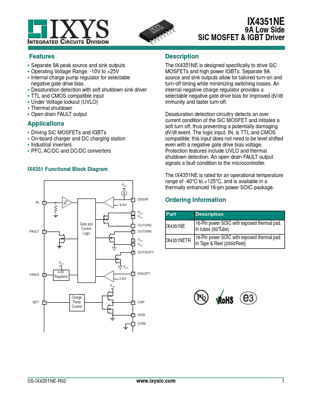
The IX4351NE is designed specifically to drive Si C MOSFETs and high power IGBTs. Separate 9A source and sink outputs allow for tailored turn-on and turn-off timing while minimizing switching losses. An internal negative charge regulator provides a selectable negative gate drive bias for improved d V/dt immunity and faster turn-off.
Desaturation detection circuitry detects an over current condition of the Si C MOSFET and initiates a soft turn off, thus preventing a potentially damaging d V/dt event. The logic input, IN, is TTL and CMOS patible; this input does not need to be level shifted even with a negative gate drive bias voltage. Protection features include UVLO and thermal shutdown detection. An open drain FAULT output signals a fault condition to the microcontroller.
The IX4351NE is rated for an operational temperature range of -40°C to +125°C, and is available in a thermally enhanced 16-pin power SOIC package.
Ordering Information
Part...