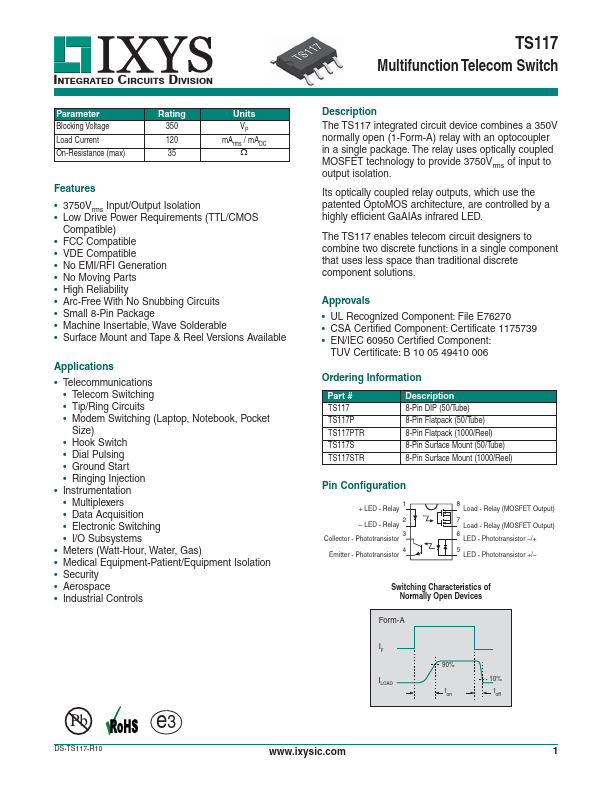
INTEGRATED CIRCUITS DIVISION
TS117
Multifunction Telecom Switch
Parameter
Blocking Voltage
Load Current
On-Resistance (max)
Rating
350
120
35
Units
VP
mArms / mADC
Features
• 3750Vrms Input/Output Isolation
• Low Drive Power Requirements (TTL/CMOS
Compatible)
• FCC Compatible
• VDE Compatible
• No EMI/RFI Generation
• No Moving Parts
• High Reliability
• Arc-Free With No Snubbing Circuits
• Small 8-Pin Package
• Machine Insertable, Wave Solderable
• Surface Mount and Tape & Reel Versions Available
Applications
• Telecommunications
• Telecom Switching
• Tip/Ring Circuits
• Modem Switching (Laptop, Notebook, Pocket
Size)
• Hook Switch
• Dial Pulsing
• Ground Start
• Ringing Injection
• Instrumentation
• Multiplexers
• Data Acquisition
• Electronic Switching
• I/O Subsystems
• Meters (Watt-Hour, Water, Gas)
• Medical Equipment-Patient/Equipment Isolation
• Security
• Aerospace
• Industrial Controls
Description
The TS117 integrated circuit device combines a 350V
normally open (1-Form-A) relay with an optocoupler
in a single package. The relay uses optically coupled
MOSFET technology to provide 3750Vrms of input to
output isolation.
Its optically coupled relay outputs, which use the
patented OptoMOS architecture, are controlled by a
highly efficient GaAIAs infrared LED.
The TS117 enables telecom circuit designers to
combine two discrete functions in a single component
that uses less space than traditional discrete
component solutions.
Approvals
• UL Recognized Component: File E76270
• CSA Certified Component: Certificate 1175739
• EN/IEC 60950 Certified Component:
TUV Certificate: B 10 05 49410 006
Ordering Information
Part #
TS117
TS117P
TS117PTR
TS117S
TS117STR
Description
8-Pin DIP (50/Tube)
8-Pin Flatpack (50/Tube)
8-Pin Flatpack (1000/Reel)
8-Pin Surface Mount (50/Tube)
8-Pin Surface Mount (1000/Reel)
Pin Configuration
1
+ LED - Relay
2
– LED - Relay
3
Collector - Phototransistor
4
Emitter - Phototransistor
8
Load - Relay (MOSFET Output)
7
Load - Relay (MOSFET Output)
6
LED - Phototransistor –/+
5
LED - Phototransistor +/–
Switching Characteristics of
Normally Open Devices
Form-A
Pb e3
I
F
ILOAD
90%
ton
10%
toff
DS-TS117-R10
www.ixysic.com
1