Datasheet4U Logo Datasheet4U.com

DE275-101N30A - RF Power MOSFET

Features

  • min. VDSS VGS(th) IGSS IDSS RDS(on) gfs TJ VGS = 0 V, ID = 3 ma VDS = VGS, ID = 250 µa VGS = ±20 VDC, VDS = 0 VDS = 0.8 VDSS TJ = 25°C VGS = 0 TJ = 125°C VGS = 15 V, ID = 0.5ID25 Pulse test, t ≤ 300µS, duty cycle d ≤ 2% VDS = 15 V, ID = 0.5ID25, pulse test typ. max. 100 V V nA µA µA Ω S +175 °C °C +175 °C °C g.
  • Isolated Substrate.
  • high isolation voltage (>2500V).
  • excellent thermal transfer.
  • Increased temperature and power.

📥 Download Datasheet

Full PDF Text Transcription (Reference)

The following content is an automatically extracted verbatim text from the original manufacturer datasheet and is provided for reference purposes only.

View original datasheet text
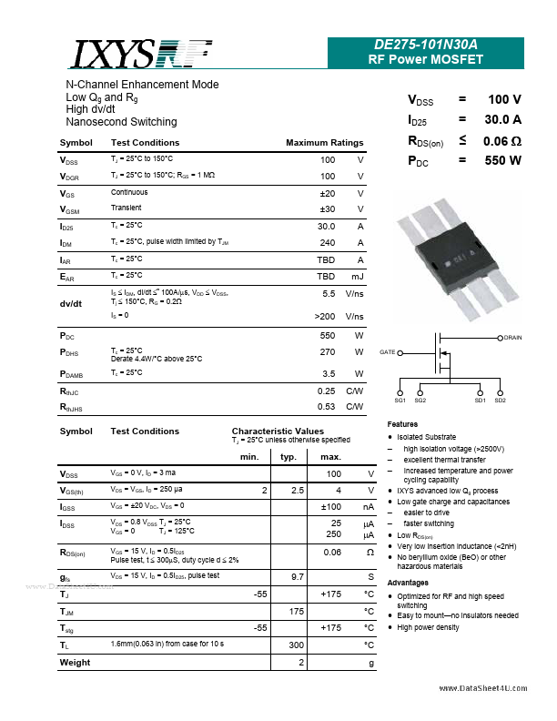
DE275-101N30A RF Power MOSFET N-Channel Enhancement Mode Low Qg and Rg High dv/dt Nanosecond Switching Symbol VDSS VDGR VGS VGSM ID25 IDM IAR EAR dv/dt Test Conditions TJ = 25°C to 150°C TJ = 25°C to 150°C; RGS = 1 MΩ Continuous Transient Tc = 25°C Tc = 25°C, pulse width limited by TJM Tc = 25°C Tc = 25°C IS ≤ IDM, di/dt ≤ 100A/µs, VDD ≤ VDSS, Tj ≤ 150°C, RG = 0.2Ω IS = 0 VDSS ID25 Maximum Ratings 100 100 ±20 ±30 30.0 240 TBD TBD 5.5 >200 550 V V V V A A A mJ V/ns V/ns W W W C/W C/W SG1 SG2 GATE = = ≤ = 100 V 30.0 A 0.06 Ω 550 W RDS(on) PDC PDC PDHS PDAMB RthJC RthJHS Symbol Test Conditions Tc = 25°C Derate 4.4W/°C above 25°C Tc = 25°C DRAIN 270 3.5 0.25 0.53 Characteristic Values TJ = 25°C unless otherwise specified SD1 SD2 Features min.
Published: |