IXTC240N055T Key Features
- easy to drive and to protect 175 °C Operating Temperature
IXTC240N055T is Power MOSFET manufactured by IXYS.
| Manufacturer | Part Number | Description |
|---|---|---|
| IXTC240N055T | N-Channel MOSFET |
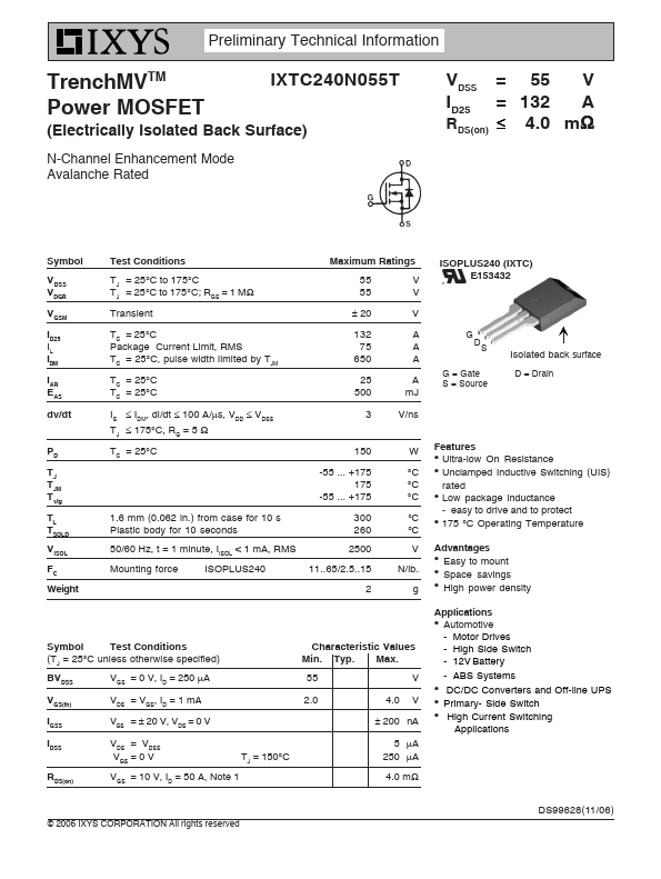
2g ISOPLUS240 (IXTC) E153432 G DS G = Gate S = Source Isolated back surface D = Drain.