IXTQ180N10T Key Features
- easy to drive and to protect 175 ° C Operating Temperature
IXTQ180N10T is Power MOSFET manufactured by IXYS.
| Manufacturer | Part Number | Description |
|---|---|---|
| IXTQ180N10T | N-ChannelMOSFET |
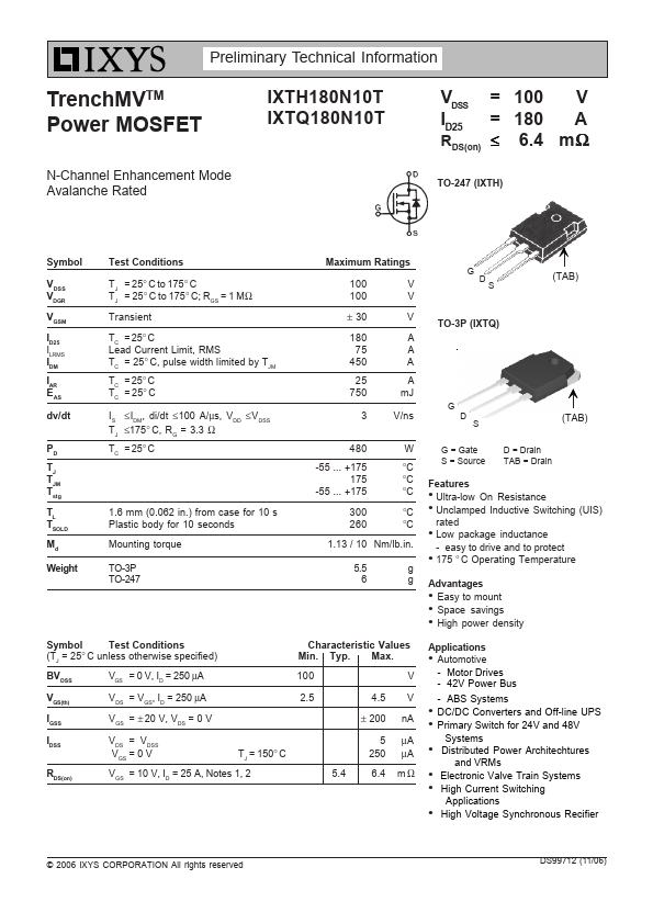
+175 °C °C °C 300 °C 260 °C 1.13 / 10 Nm/lb.in. 5.5 g 6g G = Gate S = Source D = Drain TAB = Drain.