2N3197 Overview
Description
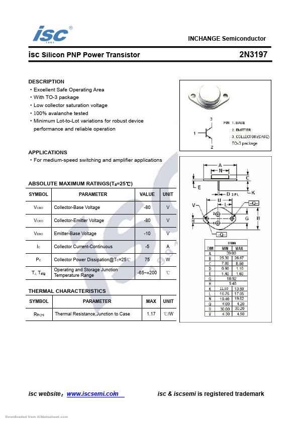
Excellent Safe Operating Area - With TO-3 package - Low collector saturation voltage - 100% avalanche tested - Minimum Lot-to-Lot variations for robust device performance and reliable operation.
| Part | 2N3197 |
|---|---|
| Description | Silicon PNP Power Transistor |
| Category | Transistor |
| Manufacturer | Inchange Semiconductor |
| Size | 224.18 KB |
Excellent Safe Operating Area - With TO-3 package - Low collector saturation voltage - 100% avalanche tested - Minimum Lot-to-Lot variations for robust device performance and reliable operation.
| Seller | Inventory | Price Breaks | Buy |
|---|---|---|---|
| No distributor offers were returned for this part. | |||
| Part Number | Manufacturer | Description |
|---|---|---|
| 2N3195 | Inchange Semiconductor | PNP Transistor |
| 2N3190 | SSDI | PNP Transistor |
| 2N3195 | SSDI | PNP Transistor |
| 2N319 | Motorola Semiconductor | PNP germanium power transistors |
| 2N3196 | SavantIC | Silicon PNP Power Transistors |