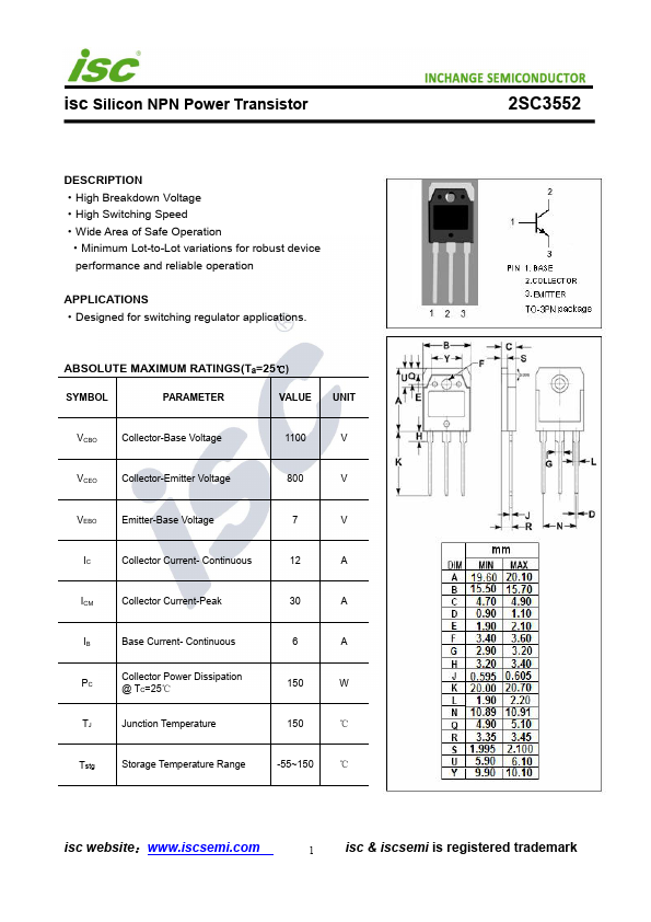
High Breakdown Voltage
High Switching Speed
Wide Area of Safe Operation
Minimum Lot-to-Lot variations for robust device performance and reliable operation
APPLICATIONS
Full PDF Text Transcription for 2SC3552 (Reference)
Note: Below is a high-fidelity text extraction (approx. 800 characters) for
2SC3552. For precise diagrams, and layout, please refer to the original PDF.
isc Silicon NPN Power Transistor DESCRIPTION ·High Breakdown Voltage ·High Switching Speed ·Wide Area of Safe Operation ·Minimum Lot-to-Lot variations for robust device p...
View more extracted text
a of Safe Operation ·Minimum Lot-to-Lot variations for robust device performance and reliable operation APPLICATIONS ·Designed for switching regulator applications. ABSOLUTE MAXIMUM RATINGS(Ta=25℃) SYMBOL PARAMETER VALUE UNIT VCBO Collector-Base Voltage 1100 V VCEO Collector-Emitter Voltage 800 V VEBO Emitter-Base Voltage 7 V IC Collector Current- Continuous 12 A ICM Collector Current-Peak 30 A IB Base Current- Continuous PC Collector Power Dissipation @ TC=25℃ TJ Junction Temperature 6 A 150 W 150 ℃ Tstg Storage Temperature Range -55~150 ℃ 2SC3552 isc website:www.iscsemi.