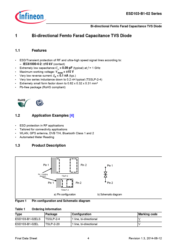
ESD103-B1-02 Description
Pin 1 Pin 2 Pin 1 Pin 1 marking (lasered) Pin 1 TSLP -2 Pin 2 Figure 1 TSSLP - 2 a) and Schematic diagram Pin 2 b) Schematic diagram Table 1 Ordering Information Type Package ESD103-B1-02ELS TSSLP-2-4 ESD103-B1-02EL TSLP-2-20 Configuration 1 line,.
ESD103-B1-02 Key Features
- IEC61000-4-2: ±10 kV (contact)
- Extremely low capacitance CL = 0.09 pF (typical) at f = 1 GHz
- Maximum working voltage: VRWM = ±15 V
- Very low reverse current: IR < 0.1 nA (typ.)
- Very low series inductance down to 0.2 nH typical (TSSLP-2-4)
- Extremely small form factor down to 0.62 x 0.32 x 0.31 mm²
- Pb-free package (RoHS pliant)
- ESD protection in RF
ESD103-B1-02 Applications
- Tailored for connectivity applications