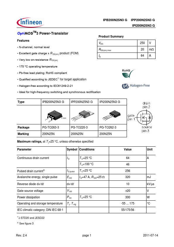
Full PDF Text Transcription for IPP200N25N3G (Reference)
Note: Below is a high-fidelity text extraction (approx. 800 characters) for
IPP200N25N3G. For precise diagrams, tables, and layout, please refer to the original PDF.
IPB200N25N3 G IPP200N25N3 G IPI200N25N3 G OptiMOSTM3 Power-Transistor Features • N-channel, normal level • Excellent gate charge x R DS(on) product (FOM) • Very low on-re...
View more extracted text
evel • Excellent gate charge x R DS(on) product (FOM) • Very low on-resistance R DS(on) • 175 °C operating temperature • Pb-free lead plating; RoHS compliant • Qualified according to JEDEC1) for target application • Halogen-free according to IEC61249-2-21 Product Summary VDS RDS(on),max ID 250 20 64 V mW A • Ideal for high-frequency switching and synchronous rectification Type IPB200N25N3 G IPP200N25N3 G IPI200N25N3 G Package Marking PG-TO263-3 200N25N PG-TO220-3 200N25N PG-TO262-3 200N25N Maximum ratings, at T j=25 °C, unless otherwise specified Parameter Continuous drain current Symbol Conditions ID T C=25 °C T C=100 °C