IPS12N03LBG
IPS12N03LBG is Power-Transistor manufactured by Infineon.
- Part of the IPD-12N comparator family.
- Part of the IPD-12N comparator family.
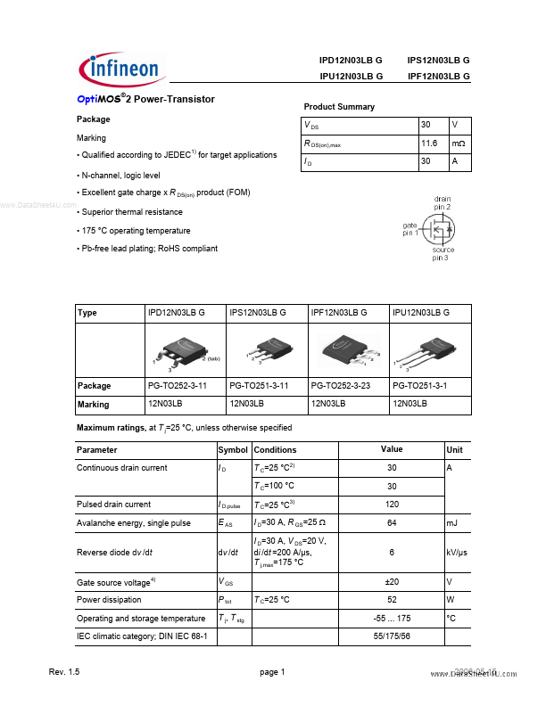
Type
IPD12N03LB G IPU12N03LB G
IPS12N03LB G IPF12N03LB G
OptiMOS®2 Power-Transistor
Package Marking
- Qualified according to JEDEC1) for target applications
- N-channel, logic level
- Excellent gate charge x R DS(on) product (FOM)
..
Product Summary V DS R DS(on),max ID 30 11.6 30 V mΩ A
- Superior thermal resistance
- 175 °C operating temperature
- Pb-free lead plating; RoHS pliant
Type
IPD12N03LB G
IPS12N03LB G
IPF12N03LB G
IPU12N03LB G
Package Marking
PG-TO252-3-11 12N03LB
PG-TO251-3-11 12N03LB
PG-TO252-3-23 12N03LB
PG-TO251-3-1 12N03LB
Maximum ratings, at T j=25 °C, unless otherwise specified Parameter Continuous drain current Symbol Conditions ID T...