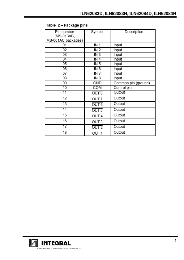
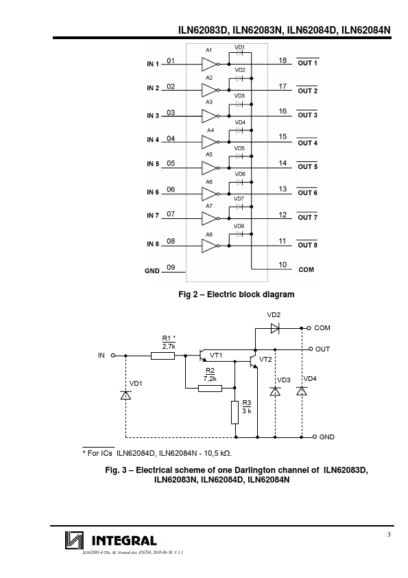
Input Input Input Input Input Input Input Input Common pin (ground) Control pin Output Output Output Output Output Output Output Output
ILN62083-4-TSe, M, Normal.dot, 456704, 2010-06-30, V 1.1
2
ILN62083D, ILN62083N, ILN62084D, ILN62084N
Fig 2
Electric block diagram
R1
2,7k IN
V
Key Features
18
MS-001AC package
1
MS-013AB package
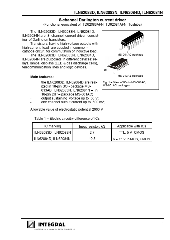
- the ILN62083D, ILN62084D are real- Fig. 1.
View of ICs in MS-001AC,
ized in 18-pin SO - package MS-
MS-001AC packages
013AB, ILN62083N, ILN62084N.
in
18-pin DIP.
package MS-001AC;
- output sustaining voltage up to 50 V;
- one channel output current up to 500 mA;
Allowable value of electrostatic potential 2000 V
Table 1.
Electric circuitry difference of ICs
IC marking ILN62083D, ILN62083N ILN62084D, ILN62084N.
Full PDF Text Transcription for ILN62083D (Reference)
Note: Below is a high-fidelity text extraction (approx. 800 characters) for
ILN62083D. For precise diagrams, and layout, please refer to the original PDF.
ILN62083D, ILN62083N, ILN62084D, ILN62084N 8-channel Darlington current driver (Functional equivalent of TD62083AFN, TD62084AFN Toshiba) The ILN62083D, ILN62083N, ILN6208...
View more extracted text
t of TD62083AFN, TD62084AFN Toshiba) The ILN62083D, ILN62083N, ILN62084D, ILN62084N are 8- channel current driver, consisting of Darlington transistors. Transistors, having high-voltage outputs with high-current load are coupled in commoncathode circuit for commutation of inductive load. The ILN62083D, ILN62083N, ILN62084D, ILN62084N are purposed in different devices: relays, lamps, displays (LED & gas discharge cells), telecommunication lines and logic devices. 18 Main features: 18 MS-001AC package 1 MS-013AB package - the ILN62083D, ILN62084D are real- Fig.