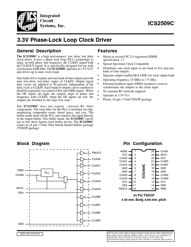
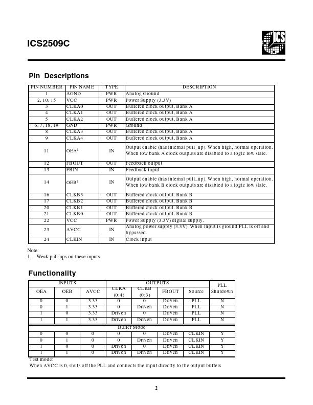
Datasheet4U Logo Datasheet4U.com

ICS2509C - 3.3V Phase-Lock Loop Clock Driver

Description

The ICS2509C is a high performance, low skew, low jitter clock driver.

It uses a phase lock loop (PLL) technology to align, in both phase and frequency, the CLKIN signal with the CLKOUT signal.

It is specifically designed for use with synchronous SDRAMs.

Features

  • Meets or exceeds PC133 registered DIMM specification 1.1 Spread Spectrum Clock Compatible Distributes one clock input to one bank of five and one bank of four outputs Separate output enable(OEA,OEB) for each output bank Operating frequency 25 MHz to 175 Mhz External feedback input (FBIN) terminal is used to synchrionize the outputs to the clock input No external RC network required Operates at 3.3V Vcc Plas.

📥 Download Datasheet

Datasheet preview – ICS2509C

Datasheet Details

Part number ICS2509C
Manufacturer Integrated Circuit Systems
File Size 248.21 KB
Description 3.3V Phase-Lock Loop Clock Driver
Datasheet download datasheet ICS2509C Datasheet
Additional preview pages of the ICS2509C datasheet.
Other Datasheets by Integrated Circuit Systems

Full PDF Text Transcription

Click to expand full text
Integrated Circuit Systems, Inc. ICS2509C 3.3V Phase-Lock Loop Clock Driver General Description The ICS2509C is a high performance, low skew, low jitter clock driver. It uses a phase lock loop (PLL) technology to align, in both phase and frequency, the CLKIN signal with the CLKOUT signal. It is specifically designed for use with synchronous SDRAMs. The ICS2509C operates at 3.3V VCC and drives up to nine clock loads. One bank of five outputs and one bank of four outputs provide nine low-skew, low-jitter copies of CLKIN. Output signal duty cycles are adjusted to 50 percent, independent of the duty cycle at CLKIN. Each bank of outputs can be enabled or disabled separately via control (OEA and OEB) inputs.
Published: |