• Part: ICS570B
  • Description: Multiplier and Zero Delay Buffer
  • Manufacturer: Integrated Circuit Systems
  • Size: 110.06 KB
Download ICS570B Datasheet PDF
ICS570B page 2
Page 2
ICS570B page 3
Page 3

ICS570B Datasheet Text

.. PRELIMINARY INFORMATION ICS570B Multiplier and Zero Delay Buffer Features - Packaged in 8 pin SOIC. - Pin-for-pin replacement and upgrade to ICS570/ICS570A - Functional equivalent to AV9170 (not a pinfor-pin replacement). - Low input to output skew of 300 ps max (>60 MHz outputs). - Low skew (100 ps) outputs. - Ability to choose between 14 different multipliers from 0.5X to 32X. - Input clock frequency up to 150 MHz at 3.3V. - Can recover degraded input clock duty cycle. - Output clock duty cycle of 45/55. - Power Down and Tri-State Mode. - Full CMOS clock swings with 25mA drive capability at TTL levels. - Advanced, low power CMOS process. - Operating voltage of 3.3 V (±5%). - Industrial temperature version available Description 
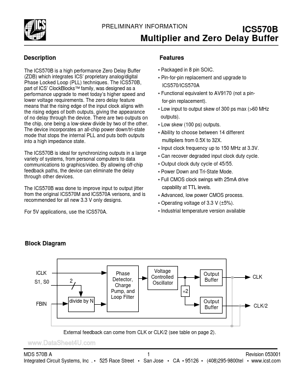
The ICS570B is a high performance Zero Delay Buffer (ZDB) which integrates ICS’ proprietary analog/digital Phase Locked Loop (PLL) techniques. The ICS570B, part of ICS’ ClockBlocks™ family, was designed as a performance upgrade to meet today’s higher speed and lower voltage requirements. The zero delay feature means that the rising edge of the input clock aligns with the rising edges of both outputs, giving the appearance of no delay through the device. There are two outputs on the chip, one being a low-skew divide by two of the other. The device incorporates an all-chip power down/tri-state mode that stops the internal PLL and puts both outputs into a high impedance state. The ICS570B is ideal for synchronizing outputs in a large variety of systems, from personal puters to data munications to graphics/video. By allowing off-chip feedback paths, the device can eliminate the delay through other devices. The ICS570B was done to improve input to output jitter from the original ICS570M and ICS570A verisons, and is...