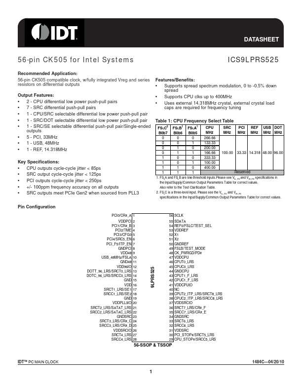
Datasheet4U Logo Datasheet4U.com

9LPRS525 - ICS9LPRS525

Product Overview

📥 Download Datasheet

Datasheet preview – 9LPRS525

Datasheet Details

Part number 9LPRS525
Manufacturer Integrated Device Technology
File Size 203.77 KB
Description ICS9LPRS525
Datasheet download datasheet 9LPRS525 Datasheet
Additional preview pages of the 9LPRS525 datasheet.

Product details

Description

PIN # PIN NAME TYPE DESCRIPTION 3.3V PCI clock output or Clock Request control A for either SRC0 or SRC2 pair The power-up default is PCI0 output, but this pin may also be used as a Clock Request control of SRC pair 0 or SRC pair 2 via SMBus.Before configuring this pin as a Clock Request Pin, the PCI output must first be disabled in byte 2, bit 0 of SMBus address space .After the PCI output is disabled (high-Z), the pin can then be set to serve as a Clock Request pin for either SRC pair 2 or p

Features

Other Datasheets by Integrated Device Technology
Published: |