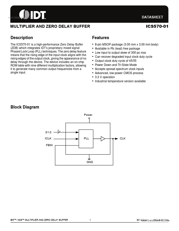
ICS570-01
ICS570-01 is MULTIPLIER AND ZERO DELAY BUFFER manufactured by Integrated Device Technology.
Description
The ICS570-01 is a high-performance Zero Delay Buffer (ZDB) which integrates IDT’s proprietary mixed signal Phased Lock Loop (PLL) techniques. The zero delay feature means that the rising edge of the input clock aligns with the rising edges of the output clock, giving the appearance of no delay through the device. The device includes an on-chip ROM table with nine different mulitplication factors, allowing it to generate many mon output frequencies from a single input.
ICS570-01 Features
- -
- -
- -
- -
- -
8-pin MSOP package (3.00 mm x 3.00 mm body) Available in Pb (lead) free package Low input to output skew of 300 ps max Can recover degraded input clock duty cycle Output clock duty cycle of 45/55 Power Down and Tri-State Mode Accepts spread spectrum clock inputs Advanced, low power CMOS process 3.3 V operation Industrial temperature version available
Block Diagram
Power
S1:0 ICLK FBIN
IDT™ / ICS™ MULTIPLIER AND ZERO DELAY BUFFER
REV B 072706
ICS570-01 MULTIPLIER AND ZERO DELAY BUFFER
..
ZDB AND MULTIPLIER
Pin Assignment
ICLK S0 GND FBIN 1 2 3 4 8 7 6 5 S1 VDD VDD CLKOUT
Pin Descriptions
Pin Number 1 2 3 4 5 6 7 8 Pin Name ICLK S0 GND FBIN CLKOUT VDD VDD S1 Pin Type Input Input Power Input Output Power Power Input Pin Description
Clock input. Select pin 0 for output clock. Connect to GND, VDD, or float per multiplier table. Connect to ground. Feedback clock input. Clock output with 5x multiplier. Connect to 3.3 V supply. Connect to 3.3 V supply. Select pin 1 for output clock. Connect to GND, VDD, or float per multiplier table.
Clock Multiplier Table
S1
0 0 0 M M M 1 1 1
S0
0 M 1 0 M 1 0 M 1
Multiplier
4x 5.333x 5x 2.5x 2x 3.333x 6x 3x 8x
ICLK Range
- 24 MHz 8
- 20 MHz 7
- 22 MHz 11
- 44 MHz 13
- 55 MHz 10
- 33 MHz...