ICS83023I
ICS83023I is 1-TO-1 DIFFERENTIAL-TOLVCMOS TRANSLATOR/BUFFER manufactured by Integrated Device Technology.
DATA SHEET
DUAL, 1-TO-1Integrated DIFFERENTIAL-TOCircuit Systems, Inc. LVCMOS TRANSLATOR/BUFFER
GENERAL DESCRIPTION
DUAL, 1-TO-1 DIFFERENTIAL-TO-LVCMOS TRANSLATOR /BUFFER
Features
- Two LVCMOS / LVTTL outputs
- Two differential CLKx, n CLKx input pairs
- CLK, n CLK pairs can accept the following differential input levels: LVDS, LVPECL, LVHSTL, SSTL, HCSL
- Maximum output frequency: 350MHz (typical)
- Output skew: 60ps (maximum)
- Part-to-part skew: 500ps (maximum)
- Additive phase jitter, RMS: 0.14ps (typical)
- Small 8 lead SOIC package saves board space
- 3.3V operating supply
- -40°C to 85°C ambient operating temperature
- Available in both standard and lead-free Ro HS-pliant packages
ICS83023I ICS83023I
The ICS83023I is a dual, 1-to-1 Differential-to IC S LVCMOS Translator/Fanout Buffer and a mem Hi Per Clock S™ ber of the Hi Per Clock S™ family of High Performance Clock Solutions from ICS. The differential inputs can accept most differential signal types (LVDS, LVHSTL, LVPECL, SSTL, and HCSL) and .. translate into two single-ended LVCMOS outputs. The small 8-lead SOIC footprint makes this device ideal for use in applications with limited board space.
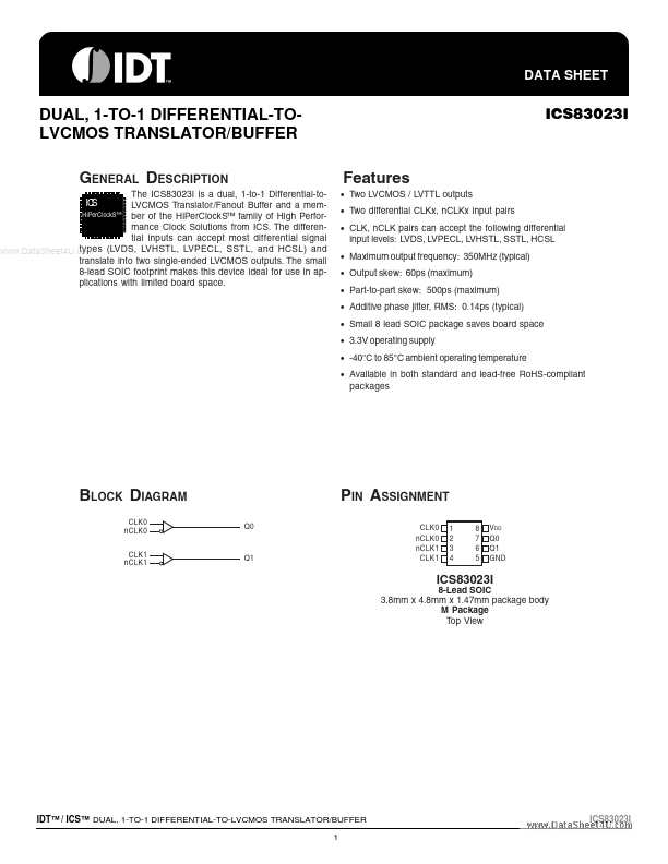
BLOCK DIAGRAM
CLK0 n CLK0 CLK1 n CLK1 Q0
PIN ASSIGNMENT
CLK0 n CLK0 n CLK1 CLK1 1 2 3 4 8 7 6 5 VDD Q0 Q1 GND
Q1
8-Lead SOIC 3.8mm x 4.8mm x 1.47mm package body M Package Top View
83023AMI
.icst./products/hiperclocks.html
REV. B JANUARY 18, 2006
IDT™ / ICS™ DUAL, 1-TO-1 DIFFERENTIAL-TO-LVCMOS TRANSLATOR/BUFFER 1
ICS83023I Circuit DUAL, 1-TO-1 DIFFERENTIAL-TO-LVCMOS TRANSLATOR/BUFFER
Integrated...