ICS831752I
Overview
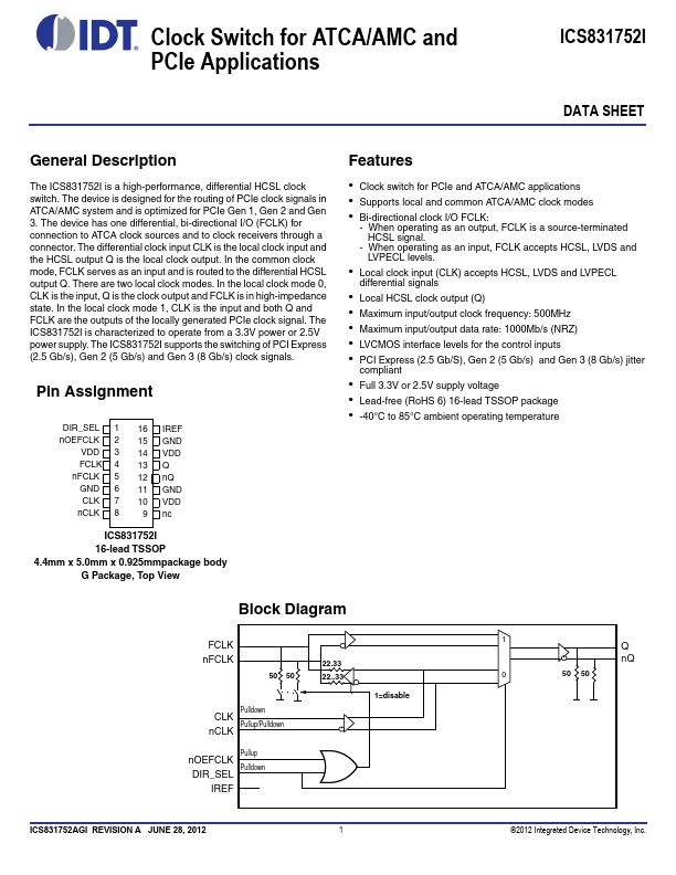
The ICS831752I is a high-performance, differential HCSL clock switch. The device is designed for the routing of PCIe clock signals in ATCA/AMC system and is optimized for PCIe Gen 1, Gen 2 and Gen 3.
- Clock switch for PCIe and ATCA/AMC applications
- Supports local and common ATCA/AMC clock modes
- Bi-directional clock I/O FCLK: - When operating as an output, FCLK is a source-terminated HCSL signal. - When operating as an input, FCLK accepts HCSL, LVDS and LVPECL levels.
- Local clock input (CLK) accepts HCSL, LVDS and LVPECL differential signals
- Local HCSL clock output (Q)
- Maximum input/output clock frequency: 500MHz
- Maximum input/output data rate: 1000Mb/s (NRZ)
- LVCMOS interface levels for the control inputs
- PCI Express (2.5 Gb/S), Gen 2 (5 Gb/s) and Gen 3 (8 Gb/s) jitter compliant
- Full 3.3V or 2.5V supply voltage