• Part: ICS83210
  • Description: 1-TO-10 HSTL FANOUT BUFFER
  • Manufacturer: Integrated Device Technology
  • Size: 204.70 KB
Download ICS83210 Datasheet PDF
Integrated Device Technology
ICS83210
ICS83210 is 1-TO-10 HSTL FANOUT BUFFER manufactured by Integrated Device Technology.
DESCRIPTION 
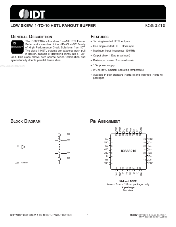
The ICS83210 is a low skew, 1-to-10 HSTL Fanout IC S Buffer and a member of the Hi Per Clock S™ Family Hi Per Clock S™ of High Performance Clock Solutions from IDT. The class II HSTL outputs are balanced push-pull in design, capable of delivering 16m A into a 10p F load. This class allows both source series termination and symmetrically double parallel termination. .. FEATURES - Ten single-ended HSTL outputs - One single-ended HSTL clock input - Maximum input frequency: 150MHz - Output skew: 110ps (maximum) - Part-to-part skew: 2ns (maximum) - 1.5V power supply - 0°C to 85°C ambient operating temperature - Available in both standard (Ro HS 5) and lead-free (Ro HS 6) packages BLOCK DIAGRAM Q0 Q1 IN Q8 Q9 n OE Pulldown PIN ASSIGNMENT 32 31 30 29 28 27 26 25 VDD GND VDD n OE GND IN VDD GND 1 2 3 4 5 6 7 8 9 10 11 12 13 14 15 16 GND GND Q9 VDD VDD Q8 Q7 GND 32-Lead TQFP 7mm x 7mm x 1.0mm package body Y package Top View Q0 Q1 Q2 24 23 22 21 20 19 18 17 GND Q3 Q4 VDD VDD Q5 Q6 GND IDT ™ / ICS™ LOW SKEW, 1-TO-10 HSTL FANOUT BUFFER ICS83210AY REV. A MAY 15, 2007 ICS83210 LOW SKEW, 1-TO-10 HSTL FANOUT BUFFER TABLE 1. PIN DESCRIPTIONS Number 1, 3, 7, 12, 13, 20, 21, 28, 29 2, 5, 8, 9, 10, 16, 17, 24, 25, 31, 32 4 Name VDD GND Power Power Type Description Power supply pins. Power supply ground. Output enable/disable input pin. When LOW, outputs Qx outputs Pulldown are enabled. When HIGH, Qx outputs are disabled low. LVCMOS/LVTTL interface levels. Single-ended reference clock input. HSTL interface levels. n O E Input 5 IN Input Q9, Q8, Q7, 11, 14, 15, .. Q6, Q5, Q4, Output Single-ended HSTL clock outputs. 18, 19, 22, 23, 26, 27, 30 Q3, Q2, Q1, Q0 NOTE: Pulldown refers to internal input resistors. See Table 2, Pin Characteristics, for typical values. TABLE 2. PIN CHARACTERISTICS Symbol CIN RPULLDOWN COUT ROUT Parameter Input Capacitance Input Pulldown Resistor Output Pin Capacitance Output Impedance Test Conditions Minimum...