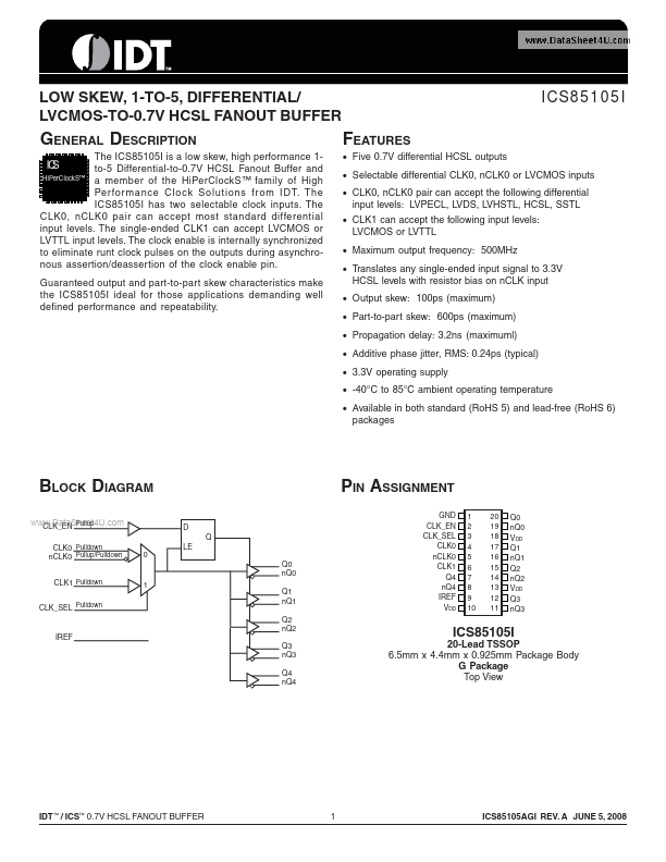
Datasheet4U Logo Datasheet4U.com

ICS85105I - DIFFERENTIAL/LVCMOS-TO-0.7V HCSL FANOUT BUFFER

Description

The ICS85105I is a low skew, high performance 1IC S to-5 Differential-to-0.7V HCSL Fanout Buffer and HiPerClockS™ a member of the HiPerClockS™ family of High Perfor mance Clock Solutions from IDT.

The ICS85105I has two selectable clock inputs.

Features

  • Five 0.7V differential HCSL outputs.
  • Selectable differential CLK0, nCLK0 or LVCMOS inputs.
  • CLK0, nCLK0 pair can accept the following differential input levels: LVPECL, LVDS, LVHSTL, HCSL, SSTL.
  • CLK1 can accept the following input levels: LVCMOS or LVTTL.
  • Maximum output frequency: 500MHz.
  • Translates any single-ended input signal to 3.3V HCSL levels with resistor bias on nCLK input.
  • Output skew: 100ps (maximum).
  • Part-to-part.

📥 Download Datasheet

Datasheet Details

Part number ICS85105I
Manufacturer Integrated Device Technology
File Size 344.39 KB
Description DIFFERENTIAL/LVCMOS-TO-0.7V HCSL FANOUT BUFFER
Datasheet download datasheet ICS85105I Datasheet
Other Datasheets by Integrated Device Technology

Full PDF Text Transcription

Click to expand full text
LOW SKEW, 1-TO-5, DIFFERENTIAL/ LVCMOS-TO-0.7V HCSL FANOUT BUFFER ICS85105I GENERAL DESCRIPTION The ICS85105I is a low skew, high performance 1IC S to-5 Differential-to-0.7V HCSL Fanout Buffer and HiPerClockS™ a member of the HiPerClockS™ family of High Perfor mance Clock Solutions from IDT. The ICS85105I has two selectable clock inputs. The CLK0, nCLK0 pair can accept most standard differential input levels. The single-ended CLK1 can accept LVCMOS or LVTTL input levels. The clock enable is internally synchronized to eliminate runt clock pulses on the outputs during asynchronous assertion/deassertion of the clock enable pin. Guaranteed output and part-to-part skew characteristics make the ICS85105I ideal for those applications demanding well defined performance and repeatability.
Published: |