Datasheet Details
| Part number | ICS854S054I |
|---|---|
| Manufacturer | Integrated Device Technology |
| File Size | 1.15 MB |
| Description | 4:1 Differential-to-LVDS Clock Multiplexer |
| Datasheet |
 ICS854S054I Datasheet ICS854S054I Datasheet
|

|
|
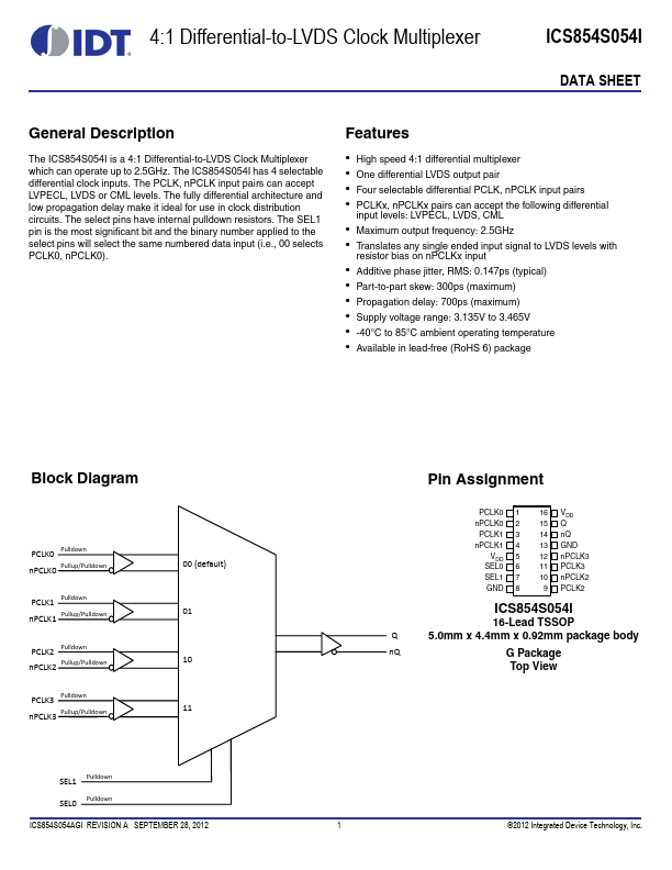
The ICS854S054I is a 4:1 Differential-to-LVDS Clock Multiplexer which can operate up to 2.5GHz.
The ICS854S054I has 4 selectable differential clock inputs.
The PCLK, nPCLK input pairs can accept LVPECL, LVDS or CML levels.
| Part number | ICS854S054I |
|---|---|
| Manufacturer | Integrated Device Technology |
| File Size | 1.15 MB |
| Description | 4:1 Differential-to-LVDS Clock Multiplexer |
| Datasheet |
ICS854S054I Datasheet
|
|
|
|
| Part Number | Description | Manufacturer |
|---|---|---|
| ICS854S054I | 4:1 Differential-to-LVDS Clock Multiplexer | Renesas |
| ICS854S058I | 8:1 Differential-to-LVDS Clock Multiplexer | Renesas |
| ICS854S006I | Differential-to-LVDS Fanout Buffer | IDT |
| ICS854S01I | 2:1 Differential-to-LVDS Multiplexer | Renesas |
| ICS854S01I | 2:1 Differential-to-LVDS Multiplexer | IDT |
| Part Number | Description |
|---|---|
| ICS854S057BI | 4:1 or 2:1 LVDS Clock Multiplexer |
| ICS854S058I | 8:1 Differential-to-LVDS Clock Multiplexer |
| ICS854S013 | 1-TO-3 DIFFERENTIAL-TO-LVDS FANOUT BUFFER |
| ICS854S204I | LVPECL FANOUT BUFFER |
| ICS85411I | 1-TO-2 DIFFERENTIAL-TO-LVDS FANOUT BUFFER |
The following content is an automatically extracted verbatim text from the original manufacturer datasheet and is provided for reference purposes only.