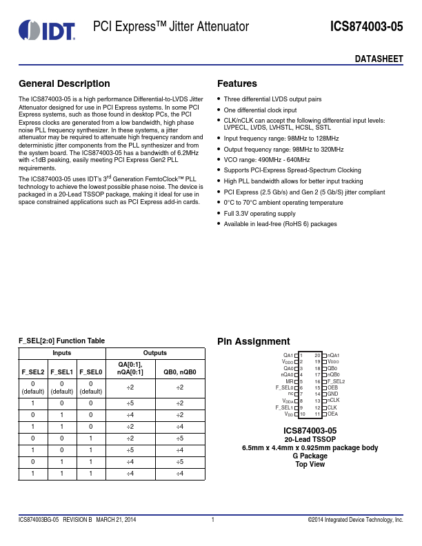
PCI Express™ Jitter Attenuator
ICS874003-05
DATASHEET
General Description
The ICS874003-05 is a high performance Differential-to-LVDS Jitter
Attenuator designed for use in PCI Express systems. In some PCI
Express systems, such as those found in desktop PCs, the PCI
Express clocks are generated from a low bandwidth, high phase
noise PLL frequency synthesizer. In these systems, a jitter
attenuator may be required to attenuate high frequency random and
deterministic jitter components from the PLL synthesizer and from
the system board. The ICS874003-05 has a bandwidth of 6.2MHz
with <1dB peaking, easily meeting PCI Express Gen2 PLL
requirements.
The ICS874003-05 uses IDT’s 3rd Generation FemtoClock™ PLL
technology to achieve the lowest possible phase noise. The device is
packaged in a 20-Lead TSSOP package, making it ideal for use in
space constrained applications such as PCI Express add-in cards.
Features
• Three differential LVDS output pairs
• One differential clock input
• CLK/nCLK can accept the following differential input levels:
LVPECL, LVDS, LVHSTL, HCSL, SSTL
• Input frequency range: 98MHz to 128MHz
• Output frequency range: 98MHz to 320MHz
• VCO range: 490MHz - 640MHz
• Supports PCI-Express Spread-Spectrum Clocking
• High PLL bandwidth allows for better input tracking
• PCI Express (2.5 Gb/s) and Gen 2 (5 Gb/S) jitter compliant
• 0°C to 70°C ambient operating temperature
• Full 3.3V operating supply
• Available in lead-free (RoHS 6) packages
F_SEL[2:0] Function Table
Inputs
F_SEL2 F_SEL1 F_SEL0
000
(default) (default) (default)
100
010
110
001
101
011
111
Outputs
QA[0:1],
nQA[0:1]
QB0, nQB0
÷2 ÷2
÷5 ÷2
÷4 ÷2
÷2 ÷4
÷2 ÷5
÷5 ÷4
÷4 ÷5
÷4 ÷4
Pin Assignment
QA1
VDDO
QA0
nQA0
MR
F_SEL0
nc
VDDA
F_SEL1
VDD
1
2
3
4
5
6
7
8
9
10
20 nQA1
19 VDDO
18 QB0
17 nQB0
16 F_SEL2
15 OEB
14 GND
13 nCLK
12 CLK
11 OEA
ICS874003-05
20-Lead TSSOP
6.5mm x 4.4mm x 0.925mm package body
G Package
Top View
ICS874003BG-05 REVISION B MARCH 21, 2014
1
©2014 Integrated Device Technology, Inc.