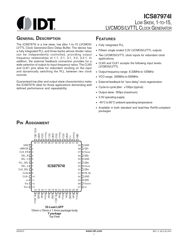
ICS87974I Description
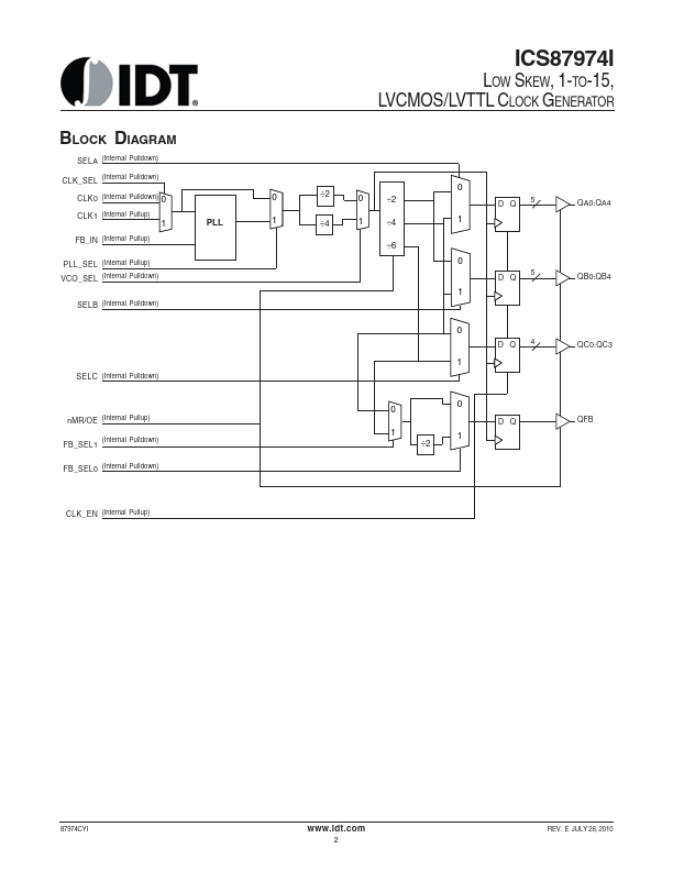
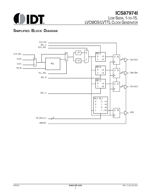
The ICS87974I is a low skew, low jitter 1-to-15 LVCMOS/ LVTTL Clock Generator/Zero Delay Buffer. In addition, the external feedback connection provides for a wide selection of output-to-input frequency ratios. The CLK0 and CLK1 pins allow for redundant clocking on the input and dynamically switching the PLL between two clock sources.
ICS87974I Key Features
- Fully integrated PLL
- Fifteen single ended 3.3V LVCMOS/LVTTL outputs
- Two LVCMOS/LVTTL clock inputs for redundant clock