ICS9LPR501 Description
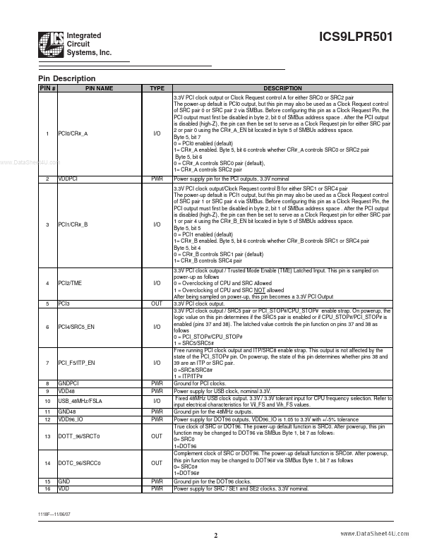
PIN # PIN NAME TYPE DESCRIPTION 3.3V PCI clock output or Clock Request control A for either SRC0 or SRC2 pair The power-up default is PCI0 output, but this pin may also be used as a Clock Request control of SRC pair 0 or SRC pair 2 via SMBus. Before configuring this pin as a Clock Request Pin, the PCI output must first be disabled in byte 2, bit 0 of SMBus add.
ICS9LPR501 Key Features
- CPU differential low power push-pull pairs
- SRC differential low power push-pull pairs
- CPU/SRC selectable differential low power push-pull pair
- SRC/DOT selectable differential low power push-pull pair
- PCI, 33MHz
- PCI_F, 33MHz free running
- USB, 48MHz
- REF, 14.318MHz Key Specifications
- CPU outputs cycle-cycle jitter < 85ps
- SRC output cycle-cycle jitter < 125ps