IDT8SLVD1204I Description
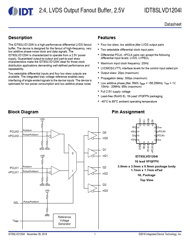
The IDT8SLVD1204I is a high-performance differential LVDS fanout buffer. The device is designed for the fanout of high-frequency, very low additive phase-noise clock and data signals. The IDT8SLVD1204I is characterized to operate from a 2.5V power supply.
IDT8SLVD1204I Key Features
- Four low skew, low additive jitter LVDS output pairs
- Two selectable differential clock input pairs
- Differential PCLK, nPCLK pairs can accept the following
- Maximum input clock frequency: 2GHz
- LVCMOS/LVTTL interface levels for the control input select pin
- Output skew: 20ps (maximum)
- Propagation delay: 300ps (maximum)
- Low additive phase jitter, RMS; fREF = 156.25MHz, VPP = 1V
- 20MHz: 95fs (maximum)
- Full 2.5V supply voltage