InterFET
Product
Folder
Technical
Support
Order
Now
J230-1
J230, J231 N-Channel JFET
Features
• InterFET N0016SH Geometry
• Low Noise: 5 nV/√Hz Typical
• Low Ciss: 4pF Typical
• RoHS Compliant
• SMT, TH, and Bare Die Package options.
Applications
• Audio Amplifiers
• Small Signal Amplifier
• Ultrahigh Impedance Pre-Amplifier
•
Description
The -40V InterFET J230 and J231 are targeted for
sensitive amplifier stages for mid-frequencies
designs. Gate leakages are typically less than 10pA
at room temperatures.
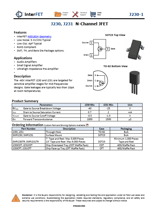
Source 1
Drain 2
Gate 3
Drain 2
Source 1
SOT23 Top View
3 Gate
TO-92 Bottom View
Product Summary
Parameters
BVGSS Gate to Source Breakdown Voltage
IDSS
Drain to Source Saturation Current
VGS(off) Gate to Source Cutoff Voltage
GFS
Forward Transconductance
J230 Min
-40
0.7
-0.5
1000
Ordering Information Custom Part and Binning Options Available
Part Number
Description
J230; J231
Through-Hole
SMPJ230; SMPJ231
Surface Mount
7“ Tape and Reel: Max 3,000 Pieces
SMPJ230TR; SMPJ231TR
13” Tape and Reel: Max 9,000 Pieces
J230COT; J231COT
Chip Orientated Tray (COT Waffle Pack)
J230CFT; J231CFT
Chip Face-up Tray (CFT Waffle Pack)
J231 Min
Unit
-25
V
2
mA
-1.5
V
1500
μS
Case
TO-92
SOT23
SOT23
COT
CFT
Packaging
Bulk
Bulk
Minimum 1,000 Pieces
Tape and Reel
400/Waffle Pack
400/Waffle Pack
Disclaimer: It is the Buyers responsibility for designing, validating and testing the end application under all field use cases and
extreme use conditions. Guaranteeing the application meets required standards, regulatory compliance, and all safety and
security requirements is the responsibility of the Buyer. These resources are subject to change without notice.
IF35020.R00