Description
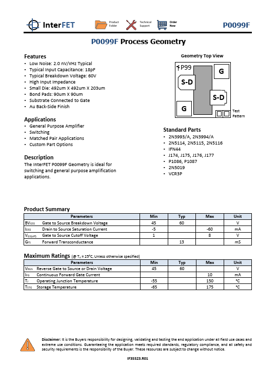
The InterFET P0099F Geometry is ideal for switching and general purpose amplification applications. Geometry Top View P99 G S-D S-D G Test Pattern Standard Parts - 2N3993/A, 2N3994/A - 2N5114, 2N5115, 2N5116 - IFN44 - J174, J175, J176, J177 - P1086, P1087 - 2N5019 - VCR3P Product Summary Parameters BVGSS Gate to Source Breakdown Voltage IDSS Drain to Source Saturation Current VGS(off) Gate to Source Cutoff Voltage GFS Forward Transconductance Min Typ Max Unit 45 60 V -5 -60 mA 1 8 V 13 mS Parameters Min Typ Max Unit VRGS Reverse Gate to Source or Drain Voltage 45 60 V IFG Continuous Forward Gate Current 10 mA TJ Operating Junction Temperature -55 150 °C TSTG Storage Temperature -65 175 °C Disclaimer: It is the Buyers responsibility for designing, validating and testing the end application under all field use cases and extreme use conditions.
Key Features
- Low Noise: 2.0 nV/√Hz Typical
- Typical Input Capacitance: 18pF
- Typical Breakdown Voltage: 60V
- High Input Impedance
- Small Die: 492um X 492um X 203um
- Bond Pads: 90um X 90um
- Substrate Connected to Gate
- Au Back-Side Finish