InterFET
Product
Folder
Technical
Support
Order
Now
J110-A
J110, J110A N-Channel JFET
Features
• InterFET N0450S Geometry
• Low Noise: 1 nV/√Hz Typical
• High Gain: 100mS Typical
• RoHS Compliant
• SMT, TH, and Bare Die Package options.
Applications
• Choppers
• Commutators
• Analog Switches
Description
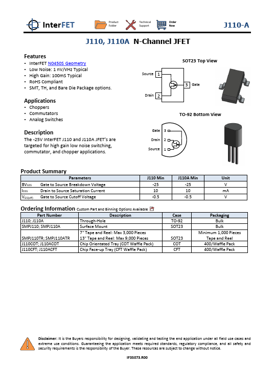
The -25V InterFET J110 and J110A JFET’s are
targeted for high gain low noise switching,
commutator, and chopper applications.
Source 1
Drain 2
SOT23 Top View
3 Gate
Gate 3
Drain 2
Source 1
TO-92 Bottom View
Product Summary
Parameters
BVGSS Gate to Source Breakdown Voltage
IDSS
Drain to Source Saturation Current
VGS(off) Gate to Source Cutoff Voltage
J110 Min
J110A Min
Unit
-25
-25
V
10
10
mA
-0.5
-0.5
V
Ordering Information Custom Part and Binning Options Available
Part Number
Description
J110; J110A
Through-Hole
SMPJ110; SMPJ110A
Surface Mount
7“ Tape and Reel: Max 3,000 Pieces
SMPJ110TR; SMPJ110ATR 13” Tape and Reel: Max 9,000 Pieces
J110COT; J110ACOT
Chip Orientated Tray (COT Waffle Pack)
J110CFT; J110ACFT
Chip Face-up Tray (CFT Waffle Pack)
Case
TO-92
SOT23
SOT23
COT
CFT
Packaging
Bulk
Bulk
Minimum 1,000 Pieces
Tape and Reel
400/Waffle Pack
400/Waffle Pack
Disclaimer: It is the Buyers responsibility for designing, validating and testing the end application under all field use cases and
extreme use conditions. Guaranteeing the application meets required standards, regulatory compliance, and all safety and
security requirements is the responsibility of the Buyer. These resources are subject to change without notice.
IF35073.R00