IR22381QPBF Overview
Description
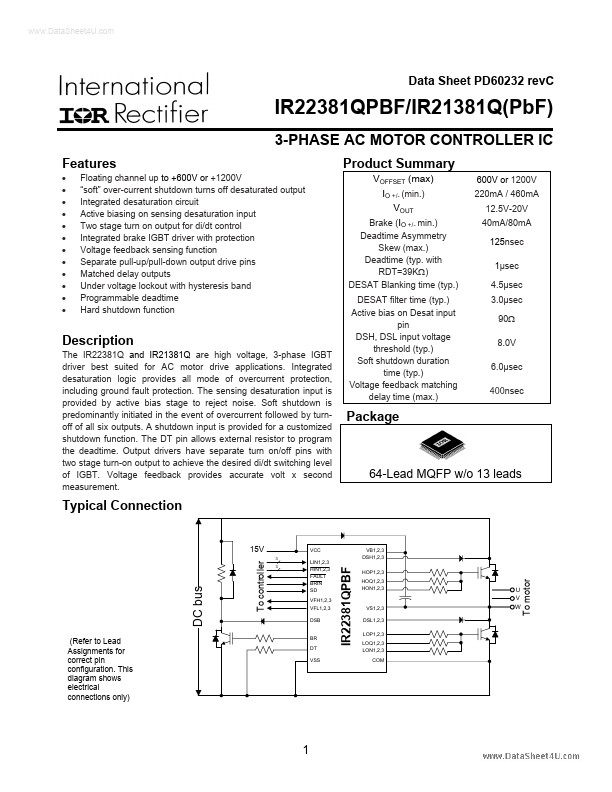
The IR22381Q and IR21381Q are high voltage, 3-phase IGBT driver best suited for AC motor drive applications. Integrated desaturation logic provides all mode of overcurrent protection, including ground fault protection.