IR22771S
Description
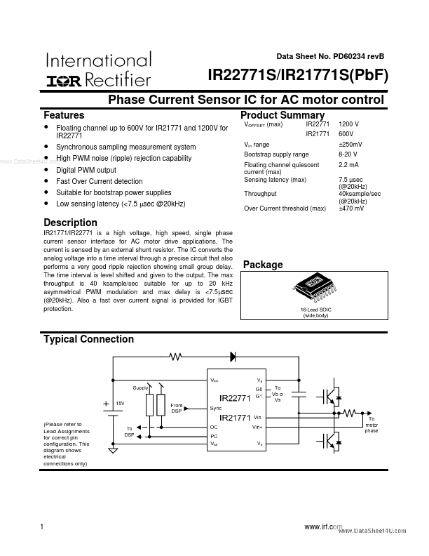
www.irf.com IR22771S/IR21771S(PbF) Timing and logic state diagrams description * See OC and PO detailed descriptions below in this document Functional block diagram Level shifter 8 PWM and OC generation www.irf.com IR22771S/IR21771S(PbF) 1 DEVICE DESCRIPTION A residual offset can be read in PO duty cycle according to VPOs (see Static electrical characteristics).
Key Features
- Floating channel up to 600V for IR21771 and 1200V for IR22771 Product Summary