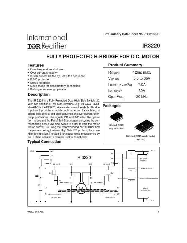
IR3220
Absolute Maximum Ratings
Absolute maximum ratings indicates sustained limits beyond which damage to the device may occur. All voltage param-
eters are referenced to Gnd lead. (TAmbient = 25oC unless otherwise specified). Symbols with (2) refer to M2 output.
Symbol
Vm1 (2)
Vin1 (2)
Vcc/gnd
I in1 (2)
Vg1 (2)
Vss
Vrc
Irc
Vdg
Idg
Isd cont.
Isd pulsed
ESD 1
ESD 2
PD
TJ max.
TL
Vcc max.
Parameter
Maximum M1 (M2) voltage (active clamp)
Maximum IN 1 (IN 2) voltage
Maximum Vcc pin to GND pin voltage
Maximum IN1 (IN 2) current
Maximum Gate 1 ( Gate 2 ) voltage
Maximum SS voltage
Maximum Vrc voltage
Maximum output current of the Vrc pin
Maximum diagnostic output voltage
Maximum diagnostic output current
Diode max. permanent current (Rth=60°C/W) (1)
(Rth=45°C/W) (1)
Diode max. pulsed current (1)
Electrostatic discharge ( human body model C=100pF, R=1500Ω)
Electrostatic discharge ( machine model C=200pF, R=0Ω, L=10µH)
Maximum power dissipation ( Rth = 60°C/W )
Max. storage & operating junction temperature
Lead temperature ( soldering 10 seconds )
Maximum Vcc voltage
Ig1 (2) max.
Ig1 (2) avg.
Maximum gate current (Ton < 5µS)
Maximum average gate current
(1) Limited by junction temperature (pulsed current limited also by internal wiring)
Min.
Vcc-37
-0.3
0.3
-1
-0.3
-0.3
-0.3
—
-0.3
-1
—
—
—
—
—
—
-40
—
—
—
—
Max.
Vcc+0.3
5.5
50
10
7.5
5.5
5.5
1
5.5
10
3.0
4.0
15
tbd
tbd
1.5
+150
300
37
100
10
Units
V
mA
V
mA
V
mA
A
V
W
°C
V
mA
Thermal Characteristics
Symbol
Parameter
Rth 1
Rth 2
Thermal junction to amb. resistance (stnd footprint 1 MOS on)
Thermal junction to ambient resistance (1" sq. footprint 1 MOS on)
Typ.
60
45
Max.
—
—
Units
°C/W
2 WWW.IRF.COM