IRF7752GPBF Overview
Key Specifications
Max Operating Temp: 150 °C
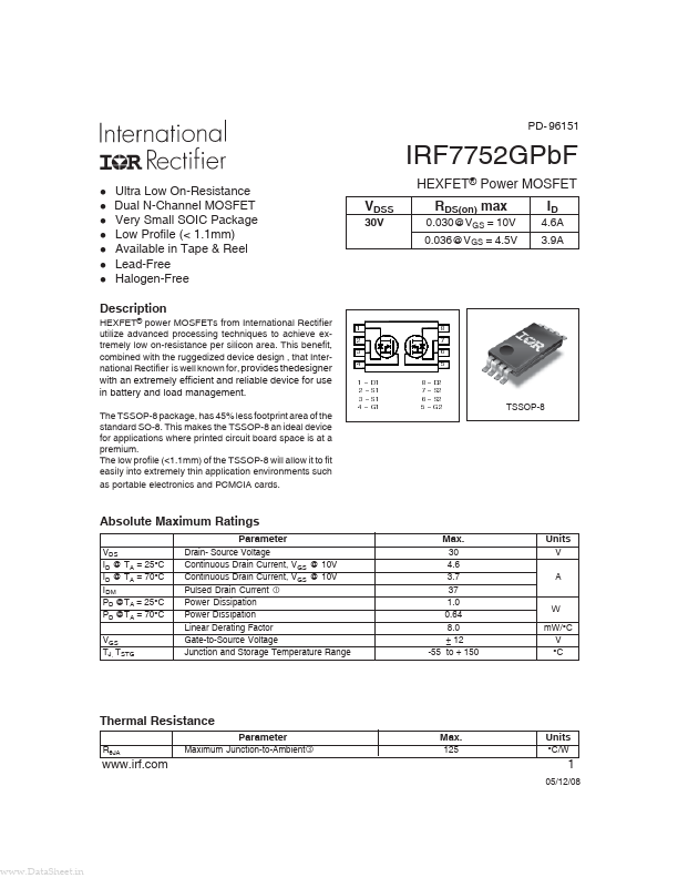
Description
HEXFET® power MOSFETs from International Rectifier utilize advanced processing techniques to achieve extremely low on-resistance per silicon area. This benefit, combined with the ruggedized device design , that International Rectifier is well known for, provides thedesigner ' !