MIL-PRF-19500
Overview
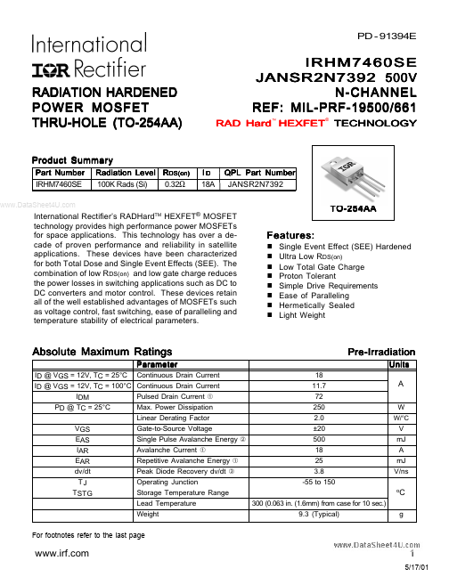
PD - 91394E RADIATION HARDENED POWER MOSFET THRU-HOLE (TO-254AA) Product Summary Part Number IRHM7460SE IRHM7460SE JANSR2N7392 500V N-CHANNEL REF: MIL-PRF-19500/661 RAD Hard HEXFET TECHNOLOGY ® ...
| Part | MIL-PRF-19500 |
|---|---|
| Description | RADIATION HARDENED POWER MOSFET |
| Category | MOSFET |
| Manufacturer | International Rectifier |
| Size | 306.19 KB |
PD - 91394E RADIATION HARDENED POWER MOSFET THRU-HOLE (TO-254AA) Product Summary Part Number IRHM7460SE IRHM7460SE JANSR2N7392 500V N-CHANNEL REF: MIL-PRF-19500/661 RAD Hard HEXFET TECHNOLOGY ® ...
| Part Number | Manufacturer | Description |
|---|---|---|
| MIL-PRF-19500 | STMicroelectronics | SEMICONDUCTOR DEVICE/ TRANSISTOR/ NPN/ SILICON/ LOW-POWER TYPES 2N2484/ 2N2484UA/ 2N2484UB/ JAN/ JANTX/ JANTXV/ JANS/ JANHC/ AND JANKC |