22346WMVEP
22346WMVEP is Quad Digitally Controlled Potentiometers manufactured by Intersil.
ISL22346WM
Quad Digitally Controlled Potentiometers (XDCP™) Low Noise, Low Power I2C Bus, 128 Taps
FN6624 Rev 1.00 November 11, 2011
The ISL22346WMVEP integrates four digitally controlled potentiometers (DCP) and non-volatile memory on a monolithic CMOS integrated circuit.
The digitally controlled potentiometers are implemented with a bination of resistor elements and CMOS switches. The position of the wipers are controlled by the user through the I2C bus interface. Each potentiometer has an associated volatile Wiper Register (WR) and a non-volatile Initial Value Register (IVR) that can be directly written to and read by the user. The contents of the WR controls the position of the wiper. At power-up, the device recalls the contents of the two DCP’s IVR to the corresponding WRs.
The DCPs can be used as a three-terminal potentiometers or as a two-terminal variable resistors in a wide variety of applications including control, parameter adjustments and signal processing.
Device Information
The specifications for an Enhanced Product (EP) device are defined in a Vendor Item Drawing (VID), which is controlled by the Defense Logistics Agency (DLA). “Hot-links” to the applicable VID and other supporting application information are provided on our website.
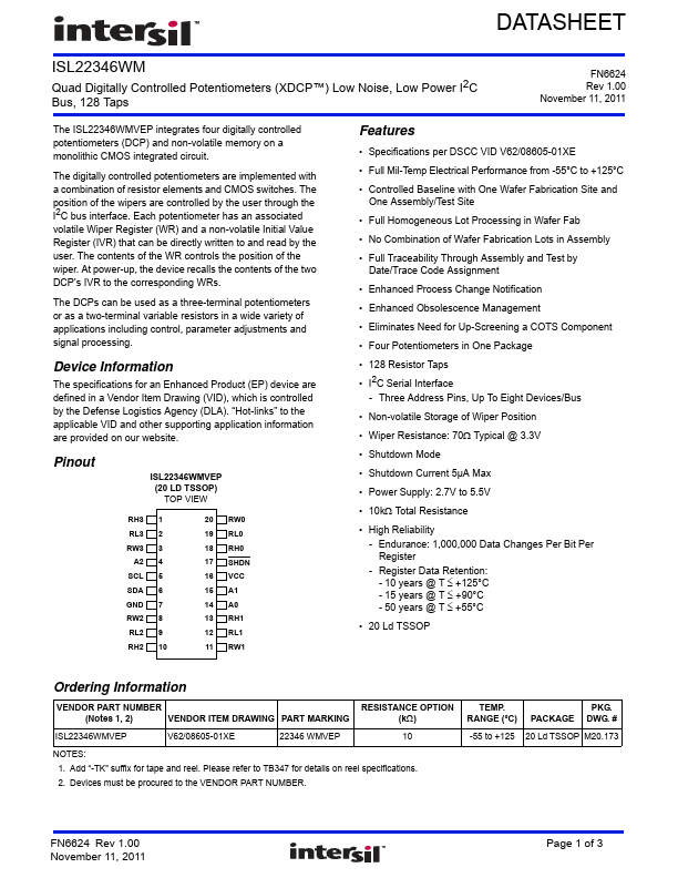
Pinout
ISL22346WMVEP (20 LD TSSOP) TOP VIEW
RH3 1 RL3 2 RW3 3
A2 4 SCL 5 SDA 6 GND 7 RW2 8 RL2 9 RH2 10
20 RW0 19 RL0 18 RH0 17 SHDN 16 VCC 15 A1 14 A0 13 RH1 12 RL1 11 RW1
Features
- Specifications per DSCC VID V62/08605-01XE
- Full Mil-Temp Electrical Performance from -55°C to +125°C
- Controlled Baseline with One Wafer Fabrication Site and One Assembly/Test Site
- Full Homogeneous Lot Processing in Wafer Fab
- No bination of Wafer Fabrication Lots in Assembly
- Full Traceability Through Assembly and Test by Date/Trace Code Assignment
- Enhanced Process Change Notification
- Enhanced Obsolescence Management
- Eliminates Need for Up-Screening a COTS ponent
- Four Potentiometers in One...