6225CA
6225CA is ISL6225CA manufactured by Intersil.
..
®
ISL6225
Data Sheet September 2003 FN9049.4
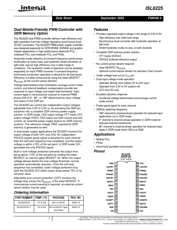
Dual Mobile-Friendly PWM Controller with DDR Memory Option
The ISL6225 dual PWM controller delivers high efficiency and tight regulation from two voltage regulating synchronous buck DC/DC converters. The ISL6225 PWM power supply controller was designed especially for DDR DRAM, SDRAM, and graphic chipset applications in high performance desknote PCs, notebook PCs, sub-notebook PCs, and PDAs. Automatic mode selection of constant-frequency synchronous rectification at heavy load, and hysteretic diode-emulation at light load, assure high efficiency over a wide range of conditions. The hysteretic mode of operation can be...