CD4023BMS
CD4023BMS is CMOS NAND Gates manufactured by Intersil.
CD4011BMS, CD4012BMS CD4023BMS
November 1994
CMOS NAND Gates
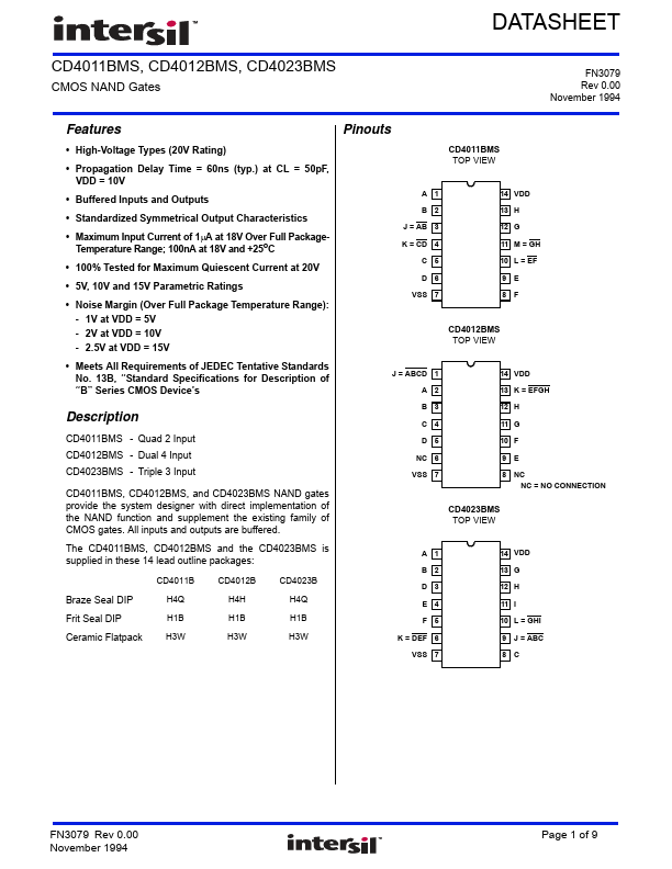
Pinouts
CD4011BMS TOP VIEW
Features
- High-Voltage Types (20V Rating)
- Propagation Delay Time = 60ns (typ.) at CL = 50pF, VDD = 10V
- Buffered Inputs and Outputs
- Standardized Symmetrical Output Characteristics
- Maximum Input Current of 1µA at 18V Over Full PackageTemperature Range; 100nA at 18V and +25oC
- 100% Tested for Maximum Quiescent Current at 20V
- 5V, 10V and 15V Parametric Ratings
A 1 B 2 J = AB 3 K = CD 4 C 5 D 6 VSS 7
14 VDD 13 H 12 G 11 M = GH 10 L = EF 9 E 8 F
- Noise Margin (Over Full Package Temperature Range):
- 1V at VDD = 5V
- 2V at VDD = 10V
- 2.5V at VDD = 15V
- Meets All Requirements of JEDEC...