Datasheet Details
| Part number | CD4073BMS |
|---|---|
| Manufacturer | Intersil (Renesas) |
| File Size | 302.22 KB |
| Description | CMOS AND Gate |
| Datasheet |
 CD4073BMS Datasheet CD4073BMS Datasheet
|
|
|
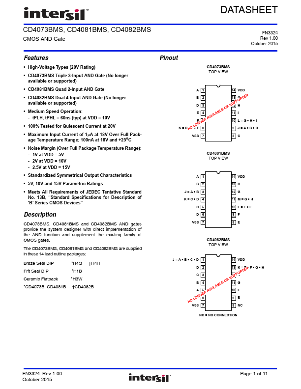
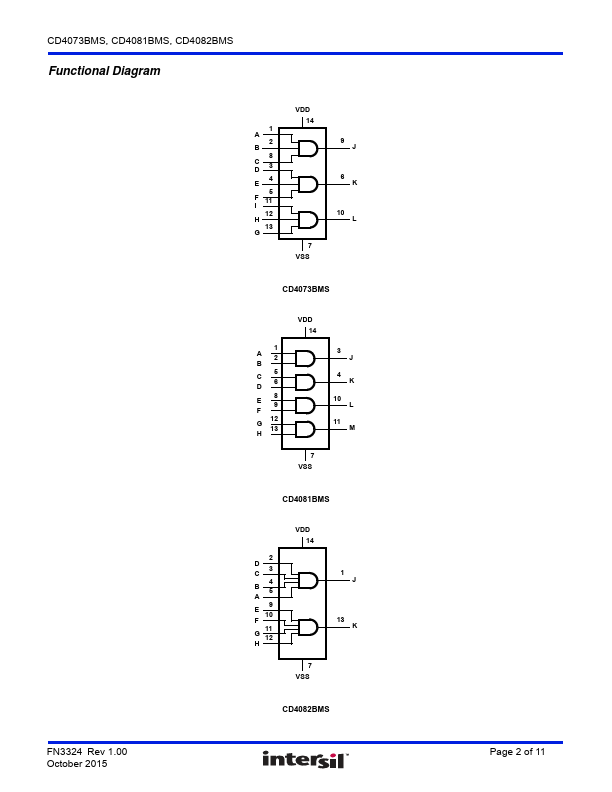
CD4073BMS, CD4081BMS and CD4082BMS AND gates provide the system designer with direct implementation of the AND function and supplement the existing family of CMOS gates.
| Part number | CD4073BMS |
|---|---|
| Manufacturer | Intersil (Renesas) |
| File Size | 302.22 KB |
| Description | CMOS AND Gate |
| Datasheet |
CD4073BMS Datasheet
|
|
|
|
| Part Number | Description | Manufacturer |
|---|---|---|
| CD4073B | CMOS AND GATES | Texas Instruments |
| CD4073B | CMOS AND Gate | RCA Solid State |
| CD4073BE | CMOS AND Gate | RCA Solid State |
| CD4070B | CMOS Quad Exclusive-OR and Exclusive-NOR Gate | RCA |
| CD4070B | CMOS Quad Exclusive-OR and Exclusive-NOR Gate | Texas Instruments |
| Part Number | Description |
|---|---|
| CD4070BMS | CMOS Quad Exclusive OR and Exclusive NOR Gates |
| CD4071BMS | CMOS OR Gate |
| CD4072BMS | CMOS OR Gate |
| CD4075BMS | CMOS OR Gate |
| CD4076BMS | CMOS 4 -Bit D-Type Registers |
The following content is an automatically extracted verbatim text from the original manufacturer datasheet and is provided for reference purposes only.