JCST CJ2101
MOSFETS
| Part No. | CJ2101 |
|---|---|
| Datasheet | CJ2101 Download |
| Manufacturer |  JCST |
| Description | MOSFETS |
| Buy | Stock & Price |
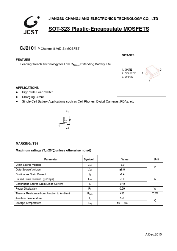
APPLICATIONS
z High Side Load Switch z Charging Circuit z Single Cell BatteryAPPLICATIONS
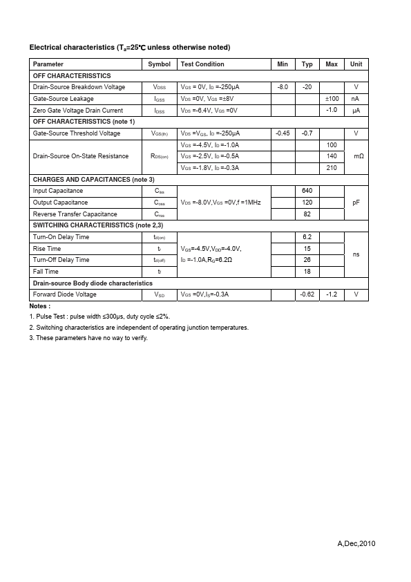
such as Cell Phones, Digital Cameras ,PDAs, etc 3 MARKING: TS1 Maximum ratings (Ta=25℃ unless otherwise noted) Parameter Drain-Source Voltage Gate-Source Voltage Continuous Drain Current Pulsed Drain Current (tp=10µs) Continuous Source-Drain Diode Current Power Dissipation Thermal Resistance from Junction to Ambient Junction Temperature Storage Temperature Symbol VDS VGS ID IDM IS PD RθJA TJ Tstg Value -8.0 ±8.0 -1.4 -3.0 -0.46 0.29 430 150 -50 ~+150 Unit V A W ℃/W ℃ A,Dec,2010 Electrical characteristics (Ta=25℃ unless otherwise noted) Parameter Symbol Test Condition OFF CHARACTERISSTICS Drain-Source Breakdown Voltage Gate-Source Leakage Zero G