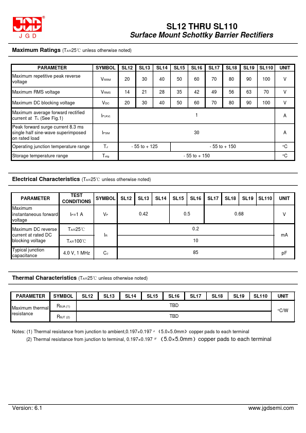
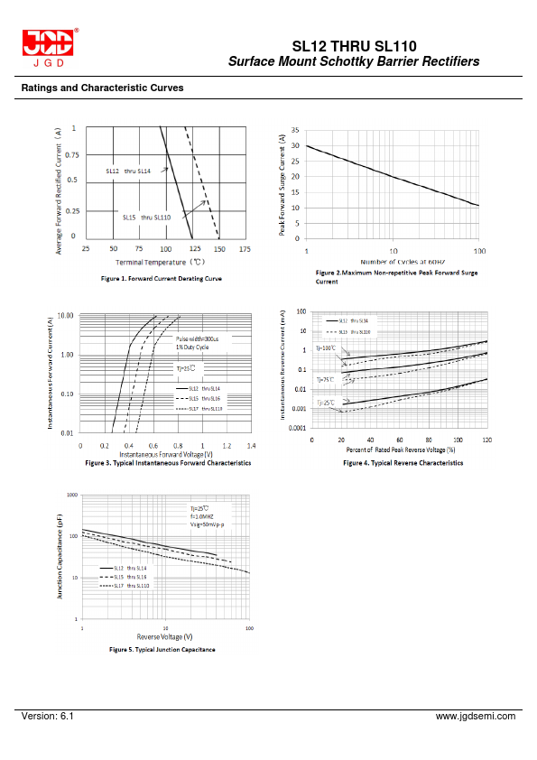
Datasheet Summary
Features
- Ideal for automated placement
- Low forward voltage drop
- Low leakage current
- Meets environmental standard MIL-S-19500D
- Moisture sensitivity:level 1, per J-STD-020
- Solder dip 260°C, 10s
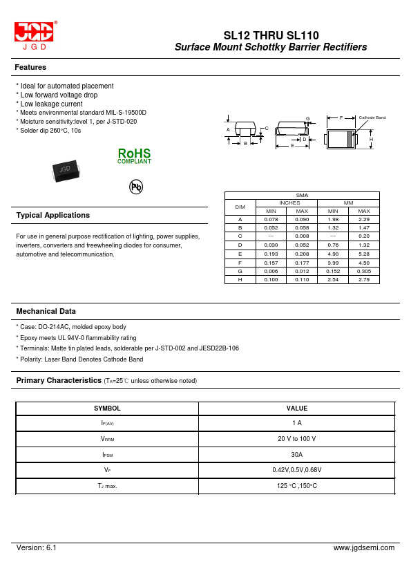
SL12 THRU SL110
Surface Mount Schottky Barrier Rectifiers
F Cathode Band H
Typical Applications
For use in general purpose rectification of lighting, power supplies, inverters, converters and freewheeling diodes for consumer, automotive and telemunication.
INCHES
MIN MAX MIN MAX
--- 0.008...