011N40P1
011N40P1 is KHB011N40P1 manufactured by KEC.
Description
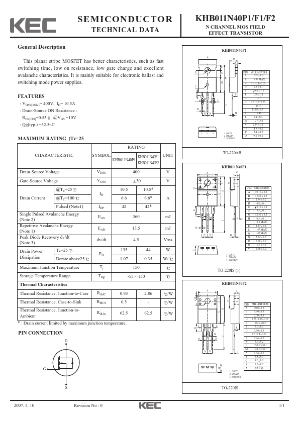
KHB011N40P1/F1/F2
N CHANNEL MOS FIELD EFFECT TRANSISTOR
KHB011N40P1
A O C F E G B Q I
DIM MILLIMETERS _ 0.2 9.9 + A B C D E
This planar stripe MOSFET has better characteristics, such as fast switching time, low on resistance, low gate charge and excellent avalanche characteristics. It is mainly suitable for electronic ballast and switching mode power supplies. FEATURES
VDSS(Min.)= 400V, ID= 10.5A Drain-Source ON Resistance : RDS(ON)=0.53 @VGS =10V Qg(typ.) =32.5n C
K M L J D N N
F G H I J
15.95 MAX 1.3+0.1/-0.05 _ 0.1 0.8 + _ 0.2 3.6 + _ 0.1 2.8 + 3.7 0.5+0.1/-0.05 1.5 _ 0.3 13.08 + 1.46 _ 0.1 1.4 + _ 0.1 1.27 + _ 0.2 2.54 + _ 0.2 4.5 + _ 0.2 2.4 + _ 0.2 9.2 +
K L M N O P Q
MAXIMUM RATING (Tc=25
RATING CHARACTERISTIC SYMBOL KHB011N40F1 UNIT KHB011N40P1 KHB011N40F2 400 30 10.5 ID 6.6 IDP EAS EAR dv/dt 135 PD 1.07 Tj Tstg 150 -55 150 0.35 W/ 42 360 13.5 4.5 44 6.6- 42- m J m J V/ns W
Q 1 2 3
1. GATE 2. DRAIN 3. SOURCE
TO-220AB
KHB011N40F1
Drain-Source Voltage Gate-Source Voltage @TC=25 Drain Current @TC=100 Pulsed (Note1) Single Pulsed Avalanche Energy (Note 2) Repetitive Avalanche Energy (Note 1) Peak Diode Recovery dv/dt (Note 3) Drain Power Dissipation Tc=25 Derate above25
VDSS VGSS
V V 10.5- A
MILLIMETERS
A B C D E F G H J K L M N O Q R
_ 0.2 10.16 + _ 0.2 15.87 + _ 0.2 2.54 + _ 0.1 0.8 + _ 0.1 3.18 + _ 0.1 3.3 + _ 0.2 12.57 + _ 0.1 0.5 + 13.0 MAX _ 0.1 3.23 + 1.47 MAX 1.47 MAX _ 0.2 2.54 + _ 0.2 6.68 + _ 0.2 4.7 + _ 0.2 2.76 +
1. GATE 2. DRAIN 3. SOURCE
Maximum Junction Temperature Storage Temperature Range Thermal Characteristics Thermal Resistance, Junction-to-Case Thermal Resistance, Case-to-Sink Thermal Resistance, Junction-to Ambient
TO-220IS (1)
KHB011N40F2
Rth JC Rth CS Rth JA
0.93 0.5 62.5
2.86...