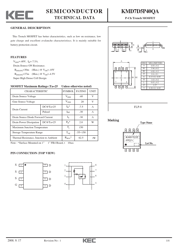
KMD7D5P40QA Description
This Trench MOSFET has better characteristics, such as low on resistance, low gate charge and excellent avalanche characteristiscs. It is mainly suitable for battery protection circuit.
KMD7D5P40QA Key Features
- 7.5 -30 -30 2.0 150 -55~150
- 24 30 m
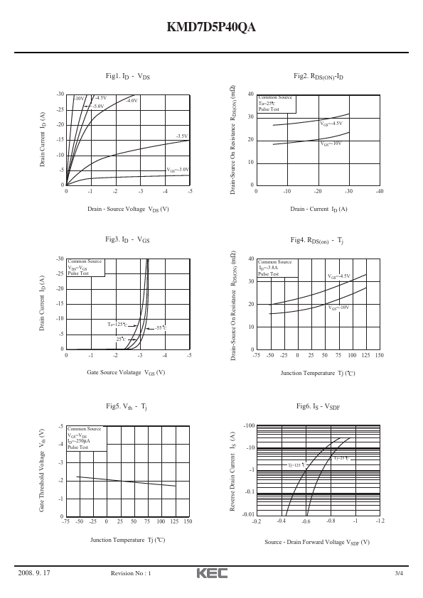
- 30 -10V -4.5V
- 25 -5.0V
- Source Voltage VDS (V)
- 30 mon Source
- 1 -2 -3
- 55 C -4
- 5 mon Source