KML0D3P20V Description
It s Mainly Suitable for Load Switching Cell Phones, Battery Powered Systems and Level-Shifter.
KML0D3P20V Key Features
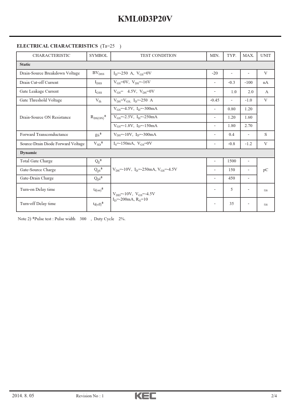
- 20 -0.45
- 450 -5
KML0D3P20V is P-Channel MOSFET manufactured by KEC.
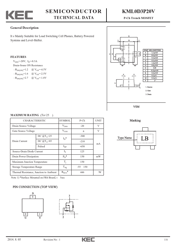
It s Mainly Suitable for Load Switching Cell Phones, Battery Powered Systems and Level-Shifter.