KKA4661
Overview
The KKA4661 is an integrated baseband delay line circuit with one line delay. It is suitable for decoders with colour-difference signal outputs ± (R-Y) and ± (B-Y).
- Two comb filters, using the switched-capacitor technique, for one line delay time (64 µS)
- 3 MHz internal clock signal derived from a 6 MHz CCO, line-locked by the sandcastle pulse (64 µS line)
- Comb filtering functions for NTSC colour-difference signals to suppress cross-colour
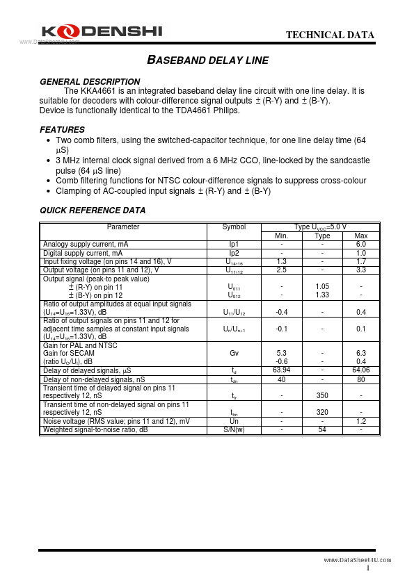
- Clamping of AC-coupled input signals ± (R-Y) and ± (B-Y) QUICK REFERENCE DATA Parameter Analogy supply current, mA Digital supply current, mA Input fixing voltage (on pins 14 and 16), V Output voltage (on pins 11 and 12), V Output signal (peak-to peak value) ± (R-Y) on pin 11 ± (B-Y) on pin 12 Ratio of output amplitudes at equal input signals (U14=U16=1.33V), dB Ratio of output signals on pins 11 and 12 for adjacent time samples at constant input signals (U14=U16=1.33V), dB Gain for PAL and NTSC Gain for SECAM (ratio UO/UI), dB Delay of delayed signals, µS Delay of non-delayed signals, nS Transient time of delayed signal on pins 11 respectively 12, nS Transient time of non-delayed signal on pins 11 respectively 12, nS Noise voltage (RMS value; pins 11 and 12), mV Weighted signal-to-noise ratio, dB Symbol Ip1 Ip2 U14,16 U11,12 U011 U012 U11/U12 Un/Un+1 Min. 1.3 2.5 -0.4 -0.1 Type UVCC=5.0 V Type 1.05 1.33 Max 6.0 1.0 1.7 3.3 0.4 0.1 Gv td tdn ttr ttrn Un S/N(w)
- 3 -0.6 63.94 40 -