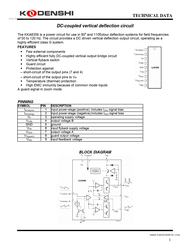
Datasheet4U Logo Datasheet4U.com

KKA8356 - DC-coupled vertical deflection circuit

General Description

Idrive(pos) Idrive(neg) VP VO(B) GND VFB VO(A) VO(guard) VI(fb) 1 2 3 4 5 6 7 8 9 input power-stage (positive);

includes II(sb) signal bias input power-stage (negative);includes II(sb) signal bias operating supply voltage output voltage B ground input flyback supply voltage output voltage A guard output voltage input feedback voltage BLOCK DIAGRAM 1 www.DataSheet4U.com KKA8356 QUICK REFERENCE DATA 3 SYMBOL PARAMETER DC supply VP supply voltage Iq quiescent supply current Vertical circuit I O(p-p) output current (peak-to-peak value) I diff(p-p) differential input current (peak-to-peak value) V diff(p-p) differential input voltage (peak-to-peak value) Flyback switch IM peak output current VFB flyback supply voltage Thermal data Tstg storage temperature Tamb operating ambient temperature Tvj virtual junction temperature MIN.

9       55 25  TYP.

Overview

www.DataSheet4U.com TECHNICAL DATA DC-coupled vertical deflection circuit The KKA8356 is a power circuit for use in 90o and 110o colour deflection systems for field frequencies of 50 to 120 Hz.

The circuit provides a DC driven vertical deflection output circuit, operating as a highly efficient class G system.

Key Features

  • Few external components.
  • Highly efficient fully DC-coupled vertical output bridge circuit.
  • Vertical flyback switch.
  • Guard circuit.
  • Protection against:.
  • short-circuit of the output pins (7 and 4).
  • short-circuit of the output pins to VP.
  • Temperature (thermal) protection.
  • High EMC immunity because of common mode inputs A guard signal in zoom mode.