Datasheet4U Logo Datasheet4U.com

2SK2111 - MOS Field Effect Transistor

Features

  • Low on-resistance RDS(on)=0.6 MAX. @VGS=4.0V,ID=0.5A High switching speed SOT-89 4.50+0.1 -0.1 1.80+0.1 -0.1 12 3 0.48+0.1 -0.1 0.53+0.1 -0.1 +0.12.50 -0.1 +0.14.00 -0.1 Unit: mm 1.50+0.1 -0.1 0.44+0.1 -0.1 +0.10.80 -0.1 +0.12.60 -0.1 3.00+0.1 -0.1 Absolute Maximum Ratings Ta = 25 Parameter Drain to source voltage Gate to source voltage Drain current Power dissipation.
  • Channel temperature Storage temperature.
  • 16 cm2X0.7mm,ceramic substrate used Symbol VDSS VGSS ID Idp PD Tch T.

📥 Download Datasheet

Datasheet preview – 2SK2111

Datasheet Details

Part number 2SK2111
Manufacturer Kexin
File Size 42.25 KB
Description MOS Field Effect Transistor
Datasheet download datasheet 2SK2111 Datasheet
Additional preview pages of the 2SK2111 datasheet.
Other Datasheets by Kexin

Full PDF Text Transcription

Click to expand full text
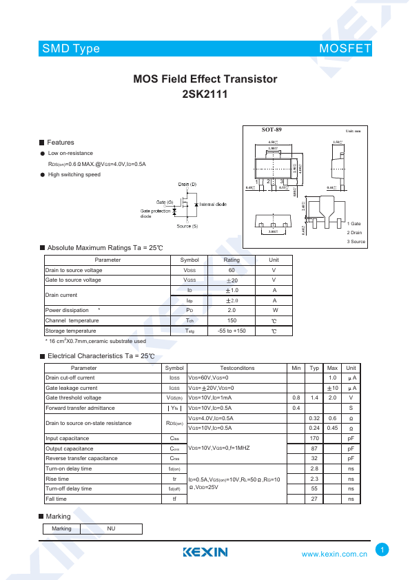
SMD Type MOS Field Effect Transistor 2SK2111 MOSFICET Features Low on-resistance RDS(on)=0.6 MAX.@VGS=4.0V,ID=0.5A High switching speed SOT-89 4.50+0.1 -0.1 1.80+0.1 -0.1 12 3 0.48+0.1 -0.1 0.53+0.1 -0.1 +0.12.50 -0.1 +0.14.00 -0.1 Unit: mm 1.50+0.1 -0.1 0.44+0.1 -0.1 +0.10.80 -0.1 +0.12.60 -0.1 3.00+0.1 -0.1 Absolute Maximum Ratings Ta = 25 Parameter Drain to source voltage Gate to source voltage Drain current Power dissipation * Channel temperature Storage temperature * 16 cm2X0.7mm,ceramic substrate used Symbol VDSS VGSS ID Idp PD Tch Tstg Rating 60 20 1.0 2.0 2.
Published: |