Full PDF Text Transcription for KQS4900 (Reference)
Note: Below is a high-fidelity text extraction (approx. 800 characters) for
KQS4900. For precise diagrams, and layout, please refer to the original PDF.
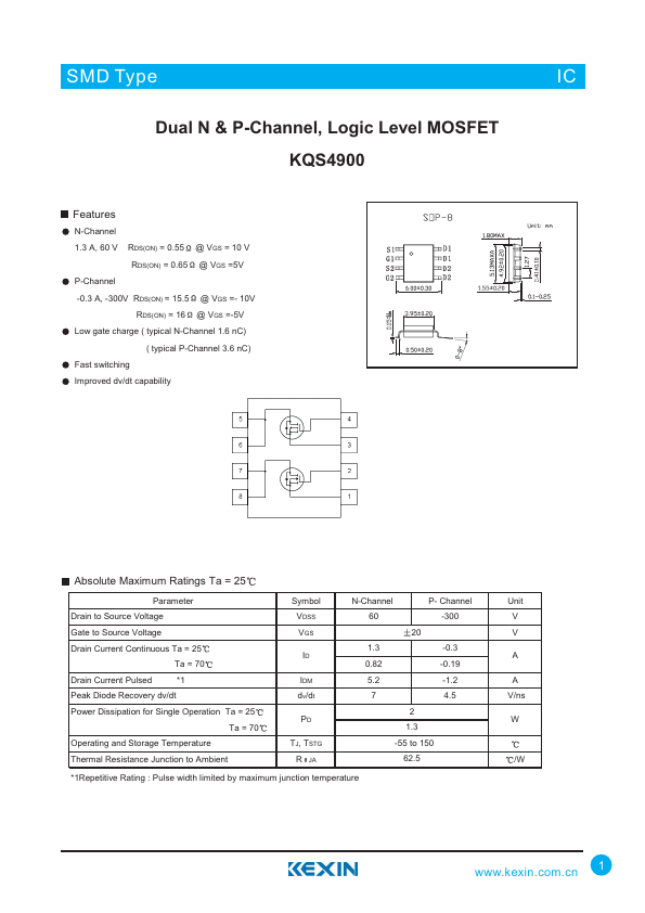
SMD Type Dual N & P-Channel, Logic Level MOSFET KQS4900 Features N-Channel 1.3 A, 60 V RDS(ON) = 0.55 @ VGS = 10 V RDS(ON) = 0.65 @ VGS =5V P-Channel -0.3 A, -300V RDS(ON...
View more extracted text
5 @ VGS = 10 V RDS(ON) = 0.65 @ VGS =5V P-Channel -0.3 A, -300V RDS(ON) = 15.5 @ VGS =- 10V RDS(ON) = 16 @ VGS =-5V Low gate charge ( typical N-Channel 1.6 nC) ( typical P-Channel 3.6 nC) Fast switching Improved dv/dt capability ICIC Absolute Maximum Ratings Ta = 25 Parameter Drain to Source Voltage Gate to Source Voltage Drain Current Continuous Ta = 25 Ta = 70 Drain Current Pulsed *1 Peak Diode Recovery dv/dt Power Dissipation for Single Operation Ta = 25 Ta = 70 Operating and Storage Temperature Thermal Resistance Junction to Ambient Symbol VDSS VGS ID IDM dv/dt PD TJ, TSTG R JA N-Channel P- Channel 60 -300 20 1.3 -0.3