KVR1333D3S8N9-2G Description
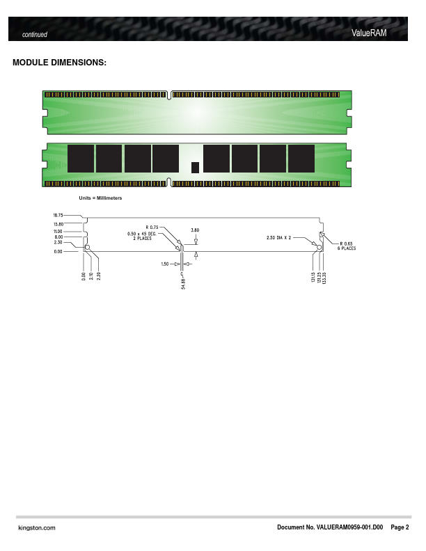
The SPD is programmed to JEDEC standard latency DDR3-1333 timing of 9-9-9 at 1.5V. This 240-pin DIMM uses gold contact fingers. The electrical and mechanical specifications are as follows:.
KVR1333D3S8N9-2G Key Features
- 2, or CL
- Power will vary depending on the SDRAM used